Download
1 / 14
140 likes | 247 Views
This document provides a detailed update on the integration and firmware implementation progress of the Trigger Board. It includes information on the input signals, firmware development, VME interface, and future plans for system testing and problem resolution.

E N D
Status of Level 1.5 Trigger Board SVD Meeting, 19-dec-2002 SVD Meeting Tom Ziegler 19-dec-2002 1
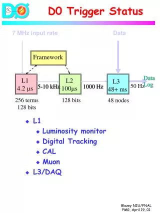
The Trigger 1.5 Board 2 bit input(ADC_start/stop) First 2 rows used in 1/10 system test Power for Trigger chips Input from 2 ADCs VME Interface 36 cablesfrom FADC 18 Trigger chips 4005 4013 PROM 8 bit trigger output SVD Meeting Tom Ziegler 19-dec-2002 2
Integration in 1/10 system test Use 1/10 system (2x(2x6) DSSDs) I use ADC_start signalto reset chips and startdata transfer from FADCs I use ADC_stop signal tosend final trigger decisionto TTM. ADC_start, ADC_stop T1.5 TTM ADC data and clock ADC_stop FADCs 2x6 DSSDs in r- 2x6 DSSDs in r-z 3 ADCs (2 used for r-z) SVD Meeting Tom Ziegler 19-dec-2002 3
Integration in 1/10 system test Thanks to various members of the SVD groupthe VME crate was set up in the local network, firm- and software modified, the 1/10 system rebuild and started up, etc… Many thanks to everybody! In the final system I’d like to have ADC_start and ADC_stop signals send from TTM to reset the chips (counters, etc.) and prepare for data transmission from FADCs and strobe and send the final trigger decision to SEQ (now I use TTM). SVD Meeting Tom Ziegler 19-dec-2002 4
Firmware VME interface chip The X4013 chip is doing all the communication from VME to/from the trigger chips. I implemented an IRQ (interrupt) system (16 data lines, where I use bit 15 as IRQ (=1), bit 14/13 as a IRQ identifier for different events and the rest of 13 bits for additional data given with IRQ (e.g. I send out the # of IRQs produced in the trigger board). => During data taking with each received IRQ monitoring data can be send out. SVD Meeting Tom Ziegler 19-dec-2002 5
Firmware VME interface chip Right now IRQ works on data lines which means,in the software running on the SPARC I am permanently reading out the 16-bit data lines in a loop which is quite CPU consuming. A problem e.g. is that IRQs get lost if CPU gets busy (the loop in the program sometimes doesn’t see an IRQ from the trigger board because the program is interrupted for some time) Later I’d like to implement that on the dedicated IRQ line of the VME (the library was not yet available in the 1/10 system) which would be a real interrupt for the CPU and should work with less CPU consumption! SVD Meeting Tom Ziegler 19-dec-2002 6
Firmware Trigger chips Descrambling of ADC data format implemented and works very nice(sorry no picture, nexttime I’ll make a printoutof the oscilloscope) Various counters are implemented (some of which will disappear in the final version as they are quite resource demanding) SVD Meeting Tom Ziegler 19-dec-2002 7
General layout of 1/10 test In the 1/10 system test no trigger logic was used as no first level trigger was available and most of the events are empty (which is not 100% true, see later). The ADC_stop signal was send back to TTM to read out the event with the FADCs via 2 PCIs. In parallel the FADC signals are decoded in the trigger board (see data format on slide before) and 32 adjecent strips are merged. This means the DSSD is devided in 16 segments and ‘1’/’0’s indicate hits/no hits in each segment. SVD Meeting Tom Ziegler 19-dec-2002 8
General layout of 1/10 test 32 strips merged to 1 segment => 16 segment bits available for each halfladder ‘0’ / ‘1’ hits => e.g. “0100000100100000” For hits in segment 2, 8 and 11! • Implemented monitoring data available: • # of interrupts produced in board • # of interrupts received in program • 16 halfladder bits ‘1’/’0’ for hits/no hits in each segment • # of hits received (each strip is counted) • # of up-going-clock in encoded data stream • 3 – 5 is available with the ID for each ADC channel SVD Meeting Tom Ziegler 19-dec-2002 9
Problems In the 1. chip I see exactly 2x the number of clock signals (??) In the moment I still count 513 clock strobes. There is one long strobe before the data transmission. (Solution implemented, not yet tested). In some of the data lines I see 1 hit, even if there are no data. (I think that is a problem with pullups, will be solved in january) I only can start ‘DAQ’ of trigger board after entering another command before. (Solution implemented, but not yet tested). I didn’t manage yet to analyze the FADC output (january) SVD Meeting Tom Ziegler 19-dec-2002 10
WEBpage I put all the important information about T1.5 (I hope) in system test on my WEB page: http://www.hep.princeton.edu/~tziegler >SVD >The subsystems: >Trigger 1.5 >1/10 system test You’ll find the description of the software, firmware, schematics, list of VME addresses used and description how to perform 1/10 system test with T1.5. SVD Meeting Tom Ziegler 19-dec-2002 11
Plan for january/february Solution of remaining problems Deeper look into comparison FADC data – Trigger monitoring data Integration into full system test. Work on online software (controling/monitoring software) Interface with T1.5 BB (=> Kirika and Gary) Did I forget something important? SVD Meeting Tom Ziegler 19-dec-2002 12
Implementation of trigger terms • Until recently the trigger logic was implemented as combinatorial logic (compilation time >24h),now I instantiated the terms explicitely in LUTs (compilation time <30min) • I did some more studies for different resolutions:e.g. resolution 16-16-32-32 compared to 32-16-16-32(better resolution in inner layers) • I also checked some event topologies (compared to single track MC) => e.g. efficiencies for bhabha events No surprises, more in january SVD Meeting Tom Ziegler 19-dec-2002 13
Everybody a merry christmas and a successful (and hopefullyless eventful) year 2003. See you all then and there! SVD Meeting Tom Ziegler 19-dec-2002 14