Download
1 / 38
380 likes | 499 Views
TK 2123 COMPUTER ORGANISATION & ARCHITECTURE. Lecture 7: CPU and Memory (3). Contents. This lecture will discuss: Cache. Error Correcting Codes. The Memory Hierarchy. Trade-off: cost, capacity and access time. Faster access time, greater cost per bit.

E N D
TK 2123COMPUTER ORGANISATION & ARCHITECTURE Lecture 7: CPU and Memory (3)
Contents • This lecture will discuss: • Cache. • Error Correcting Codes.
The Memory Hierarchy • Trade-off: cost, capacity and access time. • Faster access time, greater cost per bit. • Greater capacity, smaller cost per bit. • Greater capacity, slower access time. Access time - the time it takes to perform a read or write operation. Memory Cycle time -Time may be required for the memory to “recover” before next access, i.e. access + recovery. Transfer Rate - rate at which data can be moved.
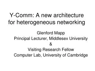
Memory Hierarchies A five-level memory hierarchy.
Hierarchy List • Registers • L1 Cache • L2 Cache • Main memory • Disk cache • Disk • Optical • Tape decreasing cost/bit, increasing capacity, and slower access time Internal memory external memory
Hierarchy List • It would be nice to use only the fastest memory, but because that is the most expensive memory, • we trade off access time for cost by using more of the slower memory. • The design challenge is to organise the data and programs in memory so that the accessed memory words are usually in the faster memory. • In general, it is likely that most future accesses to main memory by the processor will be to locations recently accessed. • So the cache automatically retains a copy of some of the recently used words from the DRAM. • If the cache is designed properly, then most of the time the processor will request memory words that are already in the cache.
Hierarchy List • No one technology is optimal in satisfying the memory requirements for a computer system. • As a consequence, the typical computer system is equipped with a hierarchy of memory subsystems; • some internal to the system (directly accessible by the processor) and • some external (accessible by the processor via an I/O module).
Cache • Small amount of fast memory • Sits between normal main memory and CPU • May be located on CPU chip or module or cache line.
Cache • The cache contains a copy of portions of main memory. • When the processor attempts to read a word of memory, a check is made to determine if the word is in the cache. • If so (hit), the word is delivered to the processor. • If not (miss), a block of main memory, consisting of some fixed number of words, is read into the cache and then the word is delivered to the processor. • Because of the phenomenon of locality of reference, when a block of data is fetched into the cache to satisfy a single memory reference, it is likely that there will be future references to that same memory location or to other words in the block. The ratio of hits to the total number of requests is known as the hit ratio.
Cache operation – overview • CPU requests contents of memory location • Check cache for this data • If present, get from cache (fast) • If not present, read required block from main memory to cache • Then deliver from cache to CPU • Cache includes tags to identify which block of main memory is in each cache slot
Cache Design • Size • Mapping Function • Replacement Algorithm • Write Policy • Block Size • Number of Caches – L1, L2, L3 etc.
Size does matter • Cost • More cache is expensive • Speed • More cache is faster (up to a point) • Checking cache for data takes time We would like the size of the cache to be small enough so that the overall average cost per bit is close to that of main memory alone and large enough so that the overall average access time is close to that of the cache alone. The larger the cache, the larger the number of gates involved in addressing the cache. The result is that large caches tend to be slightly slower than small ones.
Processor Type Year of Introduction L1 cachea L2 cache L3 cache Comparison of Cache Sizes IBM 360/85 Mainframe 1968 16 to 32 KB — — PDP-11/70 Minicomputer 1975 1 KB — — VAX 11/780 Minicomputer 1978 16 KB — — IBM 3033 Mainframe 1978 64 KB — — IBM 3090 Mainframe 1985 128 to 256 KB — — Intel 80486 PC 1989 8 KB — — Pentium PC 1993 8 KB/8 KB 256 to 512 KB — PowerPC 601 PC 1993 32 KB — — PowerPC 620 PC 1996 32 KB/32 KB — — PowerPC G4 PC/server 1999 32 KB/32 KB 256 KB to 1 MB 2 MB IBM S/390 G4 Mainframe 1997 32 KB 256 KB 2 MB IBM S/390 G6 Mainframe 1999 256 KB 8 MB — Pentium 4 PC/server 2000 8 KB/8 KB 256 KB — IBM SP High-end server/ supercomputer 2000 64 KB/32 KB 8 MB — CRAY MTAb Supercomputer 2000 8 KB 2 MB — Itanium PC/server 2001 16 KB/16 KB 96 KB 4 MB SGI Origin 2001 High-end server 2001 32 KB/32 KB 4 MB — Itanium 2 PC/server 2002 32 KB 256 KB 6 MB IBM POWER5 High-end server 2003 64 KB 1.9 MB 36 MB CRAY XD-1 Supercomputer 2004 64 KB/64 KB 1MB — a Two values seperated by a slash refer to instruction and data caches b Both caches are instruction only; no data caches
Cache: Mapping Function • Cache lines < main memory blocks: • An algorithm is needed for mapping main memory blocks into cache lines. • Three techniques: • Direct • Associative • set associative
Direct Mapping • Each block of main memory maps to only one cache line • i.e. if a block is in cache, it must be in one specific place. • pros & cons • Simple • Inexpensive • Fixed location for given block • If a program accesses 2 blocks that map to the same line repeatedly, cache misses are very high
Associative Mapping • A main memory block can load into any line of cache • Memory address is interpreted as tag and word • Tag uniquely identifies block of memory • Every line’s tag is examined for a match • Disadvantage: • Cache searching gets expensive • The complex circuitry is required to examine the tags of all cache lines in parallel.
Set Associative Mapping • A compromise that exhibits the strengths of both the direct and associative approaches while reducing their disadvantages. • Cache is divided into a number of sets. • Each set contains a number of lines. • A given block maps to any line in a given set • e.g. Block B can be in any line of set i. • With fully associative mapping, the tag in a memory address is quite large and must be compared to the tag of every line in the cache. • With k-way set associative mapping, the tag in a memory address is much smaller and is only compared to the k tags within a single set.
Replacement Algorithms • When cache memory is full, some block in cache memory must be selected for replacement. • Direct mapping : • No choice • Each block only maps to one line • Replace that line
Replacement Algorithms (2)Associative & Set Associative • Hardware implemented algorithm (speed) • Least Recently used (LRU) • An LRU algorithm, keeps track of the usage of each block and replaces the block that was last used the longest time ago. • First in first out (FIFO) • replace block that has been in cache longest • Least frequently used (LFU) • replace block which has had fewest hits • Random
Write Policy • Issues: • Must not overwrite a cache block unless main memory is up to date • Multiple CPUs may have individual caches • I/O may address main memory directly
Write through • All writes go to main memory as well as cache • Multiple CPUs can monitor main memory traffic to keep local (to CPU) cache up to date • Disadvantage: • Lots of traffic • Slows down writes • Create a bottleneck.
Cache: Line Size • As the block size increases from very small to larger sizes, the hit ratio will at first increase because of the principle of locality. • Two issues: • Larger blocks reduce the number of blocks that fit into a cache. Because each block fetch overwrites older cache contents, a small number of blocks results in data being overwritten shortly after they are fetched. • As a block becomes larger, each additional word is farther from the requested word, therefore less likely to be needed in the near future.
Number of Caches • Multilevel Caches: • On-chip cache: • A cache on the same chip as the processor. • Reduces the processor’s external bus activity and therefore speeds up execution times and increases overall system performance. • external cache: Is it still desirable? • Yes - most contemporary designs include both on-chip and external caches. • E.g. two-level cache, with the internal cache (L1) and the external cache (L2). Why? • If there is no L2 cache and the processor makes an access request for a memory location not in the L1 cache, then the processor must access DRAM or ROM memory across the bus – poor performance.
Number of Caches • More recently, it has become common to split the cache into two: • one dedicated to instructions and one dedicated to data. • There are two potential advantages of a unified cache: • For a given cache size, a unified cache has a higher hit rate than split caches because it balances the load between instruction and data fetches automatically. • Only one cache needs to be designed and implemented. • The trend is toward split caches, such as the Pentium and PowerPC, which emphasize parallel instruction execution and the prefetching of predicted future instructions. Advantage: • It eliminates contention for the cache between the instruction fetch/decode unit and the execution unit.
Problem Solution Processor on which feature first appears Intel Cache Evolution External memory slower than the system bus. Add external cache using faster memory technology. 386 Increased processor speed results in external bus becoming a bottleneck for cache access. Move external cache on-chip, operating at the same speed as the processor. 486 Internal cache is rather small, due to limited space on chip Add external L2 cache using faster technology than main memory 486 Contention occurs when both the Instruction Prefetcher and the Execution Unit simultaneously require access to the cache. In that case, the Prefetcher is stalled while the Execution Unit’s data access takes place. Create separate data and instruction caches. Pentium Increased processor speed results in external bus becoming a bottleneck for L2 cache access. Create separate back-side bus that runs at higher speed than the main (front-side) external bus. The BSB is dedicated to the L2 cache. Pentium Pro Move L2 cache on to the processor chip. Pentium II Some applications deal with massive databases and must have rapid access to large amounts of data. The on-chip caches are too small. Add external L3 cache. Pentium III Move L3 cache on-chip. Pentium 4
Locality • Page 129: Stalling.
Memory Packaging and Types A SIMM holding 256 MB. Two of the chips control the SIMM. • A group of chips, typically 8 or 16, is mounted on a tiny PCB and sold as a unit. • SIMM - single inline memory module, has a row of connectors on one side. • DIMM – Dual inline memory module, has a row of connectors on both side.
Error Correction • Hard Failure • Permanent defect • Caused by harsh environmental abuse, manufacturing defects, and wear. • Soft Error • Random, non-destructive • No permanent damage to memory • Caused by power supply problems. • Detected using Hamming error correcting code.
Error Correction • When reading out the stored word, a new set of K code bits is generated from M data bits and compared with fetch code bits. Results: • No errors – the fetch data bits are sent out. • An error is detected, and it is possible to correct the error. • Data bits + error correction bits corrector sent out the corrected set of M bits. • An error is detected, but it is not possible to correct the error. This condition is reported.
Error Correcting Code Function A function to produce code Stored codeword: M+K bits
Error Correction • Page 73, 74, 75 Tanenbaum.
Error Correcting Codes (1) Number of check bits for a code that can correct a single error
Error Correcting Codes (2) (a) Encoding of 1100 (b) Even parity added (c) Error in AC
Error Correcting Codes (3) Construction of the Hamming code for the memory word 11110000010101110 by adding 5 check bits to the 16 data bits.