Download
1 / 21
220 likes | 358 Views
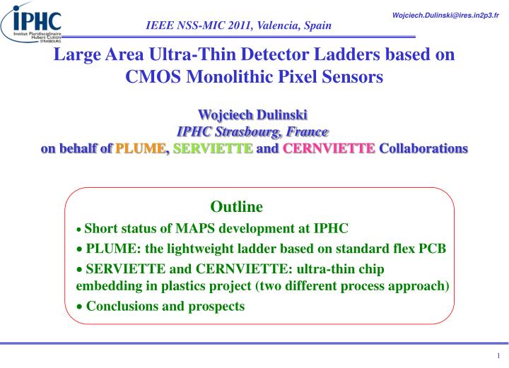
Large Area Ultra-Thin Detector Ladders based on CMOS Monolithic Pixel Sensors. Wojciech Dulinski IPHC Strasbourg, France on behalf of PLUME , SERVIETTE and CERNVIETTE Collaborations. Outline Short status of MAPS development at IPHC

E N D
Large Area Ultra-Thin Detector Ladders based on CMOS Monolithic Pixel Sensors WojciechDulinski IPHC Strasbourg, France on behalf of PLUME, SERVIETTE and CERNVIETTE Collaborations • Outline • Short status of MAPS development at IPHC • PLUME: the lightweight ladder based on standard flex PCB • SERVIETTE and CERNVIETTE: ultra-thin chip embedding in plastics project (two different process approach) • Conclusions and prospects
R.T. Monolithic Active Pixel Sensor: effective use of a thin epitaxial layer (10 – 20 µm) for MIP tracking past present Industrial availability of high resistivity substrate (epi) in a standard CMOS process Fast and more efficient charge collection radiation tolerant MAPS
Present status of MAPS: just two examples of mature designs • Binary, sparsified readout sensor for EUDET beam telescope > 2 cm2 active area, 0.7 Mpixel tracker • Medium speed readout (100 µm integration 10 kFrame/s) • Spatial resolution < 4 µm for a pitch of 18.4 µm • Efficiency for MIP > 99.5 % • Fake hit rate < 10-6 • Radiation hardness > 1013 n/cm2 (high resistivity epi substrate) • Easy to use, “off-shell” product: used already in several application • Ultimate: 4 cm2 sensor for STAR Microvertex upgrade • similar measured tracking performance as Mimosa26 • Radiation hardness >1014 n/cm2 with CMOS MAPS • attainable? • First indications: yes! Mimosa 26
One of the main feature of MAPS Potentially extremely thin (~25 µm of silicon in total, ~0.027 % X0), flexible (!) and still fully efficient for MIP tracking! Problem: how to handle, interconnect and at the end built a low mass ladder with such a thin device?
First real scale exercise: new STAR Microvertex Detector Data taking (1/4 of detector) expected in 2013, full detector installation in 2014 Estimated 0.37% X0/ladder. Can we do better?
Three RD mini-collaborations initiated by IPHC ~2 years ago, in order to develop new methods of ultra-thin ladders construction PLUME, SERVIETTE and CERNVIETTE Collaborations 1IPHC/IN2P3 Strasbourg, France 5University of Bristol, UK 6DESY, Hamburg, Germany 7University of Oxford, UK 2IMEC, Leuven, Belgium 3CMST, University of Gent, Belgium 4IFK, Goethe University, Frankfurt/M, Germany 8CERN, Geneva
PLUME concept: double-sided ladder (ILC compatible) • 2x6 Mimosa26 sensors thinned down to 50 µm • Standard double-side kapton PCB: Cu conductor (20 µm/layer) • SiC foam (8%) for spacer between layers • Estimated 0.6 % X0/two sensor layers
PLUME prototype: assembling steps bare low mass cable bare low mass cable module with 6 sensors complete ladder(2 modules)
Heat dissipation: moderate air blow seems to solve a lot of “hot spots” problems Electrical parameters (threshold dispersion, fake hit rate) almost unchanged…
Current status of PLUME prototype: ready for beam tests next week!
SERVIETTE project: use of UTCP by IMEC… • Stands for : • ULTRA THIN FILM CHIP PACKAGING • In short : • Off-the-shelf die • Thinned down to ± 20-30 µm • Packaged between two polyimide foils • Metallisation : fan-out • Circuit contact through vias Polyimide 2 • Result : • Flexible package, no wire bonding • Thin : 50-70 µm • Embeddable in commercial flexible PCB Polyimide 1 - Partner restricted PTW Oct. 2010 - HUMAN++
UTCP flow: overview • Polyimide on rigid carrier with release layer (KCl) • Dispense/spin of BCB • Chip thinning • Placement (face up) of IC 60 mm • Photo definable polyimide spinning (20µm)) • Opening vias using lithography • Cleaning of contact pads • Metallization: TiW (50nm) + Cu(1µm) • Electroplating : Cu (5µm) • Lithography to pattern metal • Encapsulation polyimide spinning • Release from carrier
First results: Mimosa18 mechanical grade sample Submitted for fabrication more thana year ago, very slow progress since, on stand-by till thinned chip placement problems solved. Aluminum conductor, multiple metal layers and multiple chips still far ahead…
CERNVIETTE: use of a “standard” flex PCB process for chip embedding in plastic foils (Rui de Oliveira, Serge Ferry) • Gluing between two kapton foils • Opening vias using lithography • Single module: intermediate tests • Metallization: Al (5-10 µm) • Lithography to pattern metal • Complete ladder assembling, laser cut along sensor edges • Gluing of another kapton foil for deposition of second metal layer 14
CERNVIETTE: stack formation Copper Polyimide Silicon chip acrylic glue 60 µm Thin layer of epoxy glue 3 to 10 µm 150 µm Acrylic glue Polyimide Acrylic glue Copper substrate 1.5mm
CERNVIETTE: processing steps 1-Gluing at 200 deg, 22kg/cm2 under vacuum 2-Photolithographic method and chemical etching by ethylene diamine to create vias on top of bonding pads 3-Plasma etching of glue in vias 4-Aluminium coating by sputtering deposition in vacuum machine
CERNVIETTE: processing steps 5-Photolithographic method and etching with phosphoric acid to pattern aluminium layer (strip, pads). • Step 1 to 5 can be repeated to create more metal layers and interconnexions • 6-Chemical Etching of copper substrate
CERNVIETTE: solid state flexible sensor wrapped over cylindrical shape (R=20 mm) and pretty well protected
Major failure: too short plasma etching of glue layer, no electrical contacts… But excellent metal adhesion and thickness uniformity! Second (corrected) iteration expected to be ready next week
CERNVIETTE: details of 4 metal layer flex (~0.12% X0) Impedance of readout lines (last metal, 100 µm width, 100 µm gap) as a function of kapton thickness: 100 Ωfor 60 µm thick kapton (last layer)
Conclusions • Construction methods of ultra-light sensor ladders are progressing rapidly, embedding in polymer seems to be a new interesting option • It is at present our preferred solution in order to take full profit from MAPS high precision tracking performances AND to equip with a reasonable budget large area detectors (replacement of silicon strips, tracking calorimeters…) Outlook • Double-sided PLUME module (0.6 % X0) fully operational, ready for beam tests starting next month. The next version (Al instead of Cu conductor, less dense SiC foam 0.3 % X0) in 2012 • Second iteration of single Mimosa26 embedded in kapton (CERNVIETTE) next week, full PLUME compatible ladder (six M26) planned for beginning of the next year • CERNVIETTE process may by much less critical, if the last metal layer on the chip is used for better (less dense) “bonding pads” distribution 7 metal CIS 0.18 µm process available! • Start to think about stitching exercise: wafer scale, up to 10x10 cm2 monolithic sensor possible