Download
1 / 14

E N D
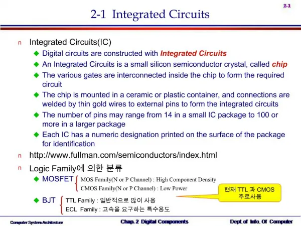
1. 2-1 Integrated Circuits Integrated Circuits(IC)
Digital circuits are constructed with Integrated Circuits
An Integrated Circuits is a small silicon semiconductor crystal, called chip
The various gates are interconnected inside the chip to form the required circuit
The chip is mounted in a ceramic or plastic container, and connections are welded by thin gold wires to external pins to form the integrated circuits
The number of pins may range from 14 in a small IC package to 100 or more in a larger package
Each IC has a numeric designation printed on the surface of the package for identification
http://www.fullman.com/semiconductors/index.html
Logic Family? ?? ??
MOSFET
BJT
2. TTL Family
54 Series : -55 � C ? 125 �C, Military
74 Series : 0 � C ? 70 � C, Commercial
54/74 : Standard
54L/74L : Low-power
54S/74S : Schottky
54LS/74LS : Low-power, Schottky
54H/74H : High-speed
CMOS Family
4000 Series(RCA), MC14500(Motorola), 5000(Toshiba), 54C/74C Series, 54HC/74HC Series
???? : -30 � C ? 85 � C , Fan-out ??, Noise Margin ??, Low-power
3. Package Types Small Outline Transistor (SOT)
5. 2-2 Decoder/Encoder Decoder
A combinational circuit that converts binary information from the n coded inputs to a maximum of 2n unique outputs
n-to-m line decoder = n x m decoder
n inputs, m outputs
If the n-bit coded information has unused bit combinations, the decoder may have less than 2n outputs
m ? 2n
3-to-8 Decoder
Logic Diagram : Fig. 2-1
Truth Table : Tab. 2-1
Commercial decoders
include one or more
Enable Input(E)
6. NAND Gate Decoder
Constructed with NAND instead of AND gates
Logic Diagram/Truth Table : Fig. 2-2
Decoder Expansion
3 X 8 Decoder constructed with two 2 X 4 Decoder
Constructed decoder : Fig. 2-3
Encoder
Inverse Operation of a decoder
2n input, n output
Truth Table : Tab. 2-2
3 OR Gates Implementation
A0 = D1 + D3 + D5 + D7
A1 = D2 + D3 + D6 + D7
A2 = D4 + D5 + D6 + D7
7. 2-3 Multiplexers Multiplexer(Mux)
A combinational circuit that receives binary information from one of 2n input data lines and directs it to a single output line
A 2n -to 1 multiplexer has 2n input data lines and
n input selection lines(Data Selector)
4-to-1 multiplexer Diagram : Fig. 2-4
4-to-1 multiplexer Function Table : Tab. 2-3
Quadruple 2-to-1 Multiplexer
Quadruple 2-to-1 Multiplexer : Fig. 2-5
8. 2-4 Registers Register
A group of flip-flops with each flip-flop capable of storing one bit of information
An n-bit register has a group of n flip-flops and is capable of storing any binary information of n bits
The simplest register consists only of flip-flops, with no external gate : Fig. 2-6
A clock input C will load all four inputs in parallel
The clock must be inhibited if the content of the register must be left unchanged
Register with Parallel Load
A 4-bit register with a load control input : Fig. 2-7
The clock inputs receive clock pulses at all times
The buffer gate in the clock input will increase �fan-out�
Load Input
1 : Four input transfer
0 : Input inhibited, Feedback from output to input(no change)
9. 2-5 Shift Registers Shift Register
A register capable of shifting its binary information in one or both directions
The logical configuration of a shift register consists of a chain of flip-flops in cascade
The simplest possible shift register uses only flip-flops : Fig. 2-8
The serial input determines what goes into the leftmost position during the shift
The serial output is taken from the output of the rightmost flip-flop
10. Bidirectional Shift Register with Parallel Load
A register capable of shifting in one direction only is called a unidirectional shift register
A register that can shift in both directions is called a bidirectional shift register
11. 2-6 Binary Counter Counter
A register goes through a predetermined sequence of state(Upon the application of input pulses)
Used for counting the number of occurrences of an event and useful for generating timing signals to control the sequence of operations in digital computers
An n-bit binary counter is a register of n flip-flop(count from 0 to 2n -1)
4 bit Synchronous Binary Counter
A counter circuit will usually employ F/F with complementing capabilities(T and J-K F/F)
4 bit Synchronous Binary Counter :
Fig. 2-10
12. Binary Counter with Parallel Load
Counters employed in digital systems(CPU Register) require a parallel load capability for transferring an initial binary number prior to the count operation
4-bit binary counter with Clear, Parallel Load, and Increment(Counter) :
Fig. 2-11
Function Table : Tab. 2-5
Clear : 1 K=X, J=0 Clear(Q=0)
(Clear, Load=X)
Load : 1 I=1 J=1, K=0
(Clear=0) I=0 J=0, K=1
Increment : 1 J=K=1(Toggle)
(Clear, Load=0)
13. 2-7 Memory Unit Memory Unit
A collection of storage cells together with associated circuits needed to transfer information in and out of storage
The memory stores binary information in groups of bits called words
Word
A group of binary information that is processed in one simultaneous operation
Byte
A group of eight bits (nibble : four bits)
The number of address line = k
Address(Identification number) : 0, 1, 2, 3, � up to 2k -1
The selection of specific word inside memory : k bit binary address
1 Kilo= 210, 1 Mega= 220, 1 Giga= 230
16 bit address line ?? : 216= 64 K
Solid State Memory(IC Memory)
RAM(Volatile Memory)
ROM(Non-volatile Memory)
14. Random Access Memory
The memory cells can be accessed for information transfer from any desired random location
Communication between a memory and its environment is achieved through data input and output lines, address selection lines, and control lines : Fig. 2-12
The two operations that a random-access memory can perform are the write and read operations
15. Read-Only Memory
A memory unit that performs the read operation only; it does not have a write capability
ROM comes with special internal electronic fuses that can be �programmed� for a specific configuration
m x n ROM : Fig. 2-13
k address input lines to select one of 2k = m words of memory, and n output lines(n bits word)
ROM is classified as a combinational circuit, because the outputs are a function of only the present inputs(address lines)
There is no need for providing storage capabilities as in a RAM
ROM is also employed in the design of control units for digital computers
A Control Unit that utilizes a ROM to store binary control information is called a micro-programmed control
Types of ROMs
UVEPROM(Chip level erase), EEPROM(Byte level erase), Flash ROM(Page or block level erase), OTPROM, Mask ROM