Download
1 / 43

E N D
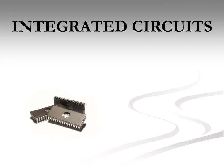
INTEGRATED CIRCUITS In electronics, an integrated circuit (also known as IC, microcircuit, microchip, silicon chip, or chip) is a miniaturized electronic circuit (consisting mainly of semiconductor devices, as well as passive components) that has been manufactured in the surface of a thin substrate of semiconductor material. Integrated circuits are used in almost all electronic equipment in use today and have revolutionized the world of electronics. The first integrated circuit was developed in the 1950s by Jack Kilby of Texas Instruments and Robert Noyce of Fairchild Semiconductor.
ADVANTAGES OF IC’S • SMALL SIZE • LOW COST • IMPROVED PERFORMANCE • HIGH RELIABILITY AND RUGGEDNESS • LOW POWER CONSUMPTION • LESS VULNERABILITY TO PARAMETER VARIATION • EASY TROUBLESHOOTING • INCREASED OPERATING SPEED • LESS WEIGHT,VOLUME • EASY REPLACEMENT
DISADVANTAGES OF IC’S • AS IC IS SMALL IN SIZE ITS UNABLE TO DISSIPATE LARGE AMOUNT OF POWER. INCREASE IN CURRENT MAY PRODUCE ENOUGH HEAT WHICH MAY DESTROY THE DEVICE. • AT PRESENT COILS, INDUCTORS AND TRANSFORMERS CAN NOT BE PRODUCED IN IC FORM.
CLASSIFICATION OF IC’S • On the basis of fabrication techniques used • On the basis of the chip size • On the basis of applications
ON BASIS OF FABRICATION • Monolithic IC’s • Thin and Thick Film IC’s. • Hybrid or Multi-chip ICs.
MONOLITHIC IC’S Monolithic circuit is built into a single stone or single crystal i.e. in monolithic ICs, all circuit components, and their interconnections are formed into or on the top of a single chip of silicon. Monolithic ICs are by far the most common type of ICs used in practice, because of mass production , lower cost and higher reliability.
THIN AND THICK FILM IC’S These devices are larger than monolithic ICs but smaller than discrete circuits. These ICs can be used when power requirement is comparatively higher. With a thin-or thick-film IC, the passive components like resistors and capacitors are integrated, but the transistors and diodes are connected as discrete components to form a complete circuit. The essential difference between the thin- and thick-film ICs is not their relative thickness but the method of deposition of film. Both have similar appearance, properties and general characteristics.
HYBRID IC’S The circuit is fabricated by interconnecting a number of individual chips. Hybrids ICs are widely used for high power audio amplifier applications . Have better performance than monolithic ICs Process is too expensive for mass production
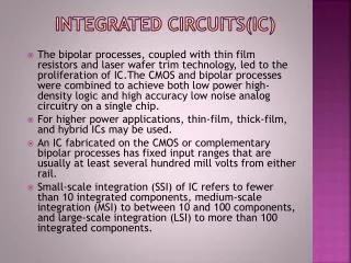
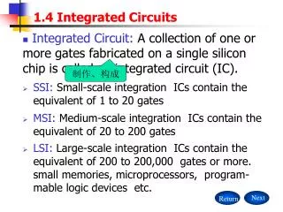
ON BASIS OF CHIP SIZE • SSI (small-scale integration) • MSI (medium-scale integration) • LSI (large-scale integration) • VLSI (very large-scale integration) • ULSI (ultra large-scale integration)
SSI AND MSI Small scale integration (SSI) has 3 to 30 gates/chip orUp to 100 electronic components per chip Medium scale integration (MSI) has 30 to 300 gates/chip or 100 to 3,000 electronic components per chip
LSI AND VLSI Large scale integration (LSI)-300 to 3,000 gates/chip or 3,000 to 100,000 electronic components per chip Very large scale integration (VLSI)-more than 3,000 gates/chip or 100,000 to 1,000,000 electronic components per chip
ULSI Ultra Large-Scale Integration (ULSI)- More than 1 million electronic components per chip The Intel 486 and Pentium microprocessors, for example, use ULSI technology. The line between VLSI and ULSI is vague.
ON BASIS OF APPLICATIONS • LINEAR INTEGRATED CIRCUITS • DIGITAL INTEGRATED CIRCUITS
When the input and output relationship of a circuit is linear, linear ICs are used. Input and output can take place on a continuous range of values. Example operational amplifiers, power amplifiers, microwave amplifiers multipliers etc. LINEAR INTEGRATED CIRCUITS
DIGITAL INTEGRATED CIRCUITS When the circuit is either in on-state or off-state and not in between the two, the circuit is called the digital circuit. ICs used in such circuits are called the digital ICs. They find wide applications in computers and logic circuits. Example logic gates, flip flops, counters, microprocessors, memory chips etc.
FABRICATION STEPS • The base on which ic is formed is a p-type substrate. • The 2nd layer is a thin layer grown as single n-type crystal and also known as epitaxial growth. Active and passive devices of the circuits are formed in this layer by diffusion. • Selective diffusion is needed at each diffusion stage.
SiO2 layer is formed on the top of epitaxial layer. • n+ emitter is diffused into p-type base by photolithographic masking and etching. • Another SiO2 layering , masking and etching exposes n+ and p areas for forming metallic contacts. • A thin Al layer is then deposited over entire chip surface leaving inter & external connections, the rest of Al is etched away.
EPITAXIAL GROWTH Epitaxial growth is the formation of layer of Si crystal with n-type doping as an extension of the existing p-type Si substrate. The process is carried in a reactor at 1000 C where finished wafers the inserted. Si is obtained by breaking SiCl4 in presence of H2 : SiCl4 + 2 H2 --> Si + 4 HCl For n-type doping of epitaxial layer PH4 & N2 is fed to the reactor .
OXIDE GROWTH SiO2 layer is grown and removed from surface of silicon slice many times during manufacture of IC’s Characteristics of SiO2 layer : • Acts as diffusion mask permitting selective diffusions into Si wafer • Used for surface passivation i.e. protecting junction from moisture and other atmospheric contaminants • Used for insulating the metal interconnections from Si
The Process… The silicon wafers are kept in quartz boat and inserted into a quartz tube. the tube is heated to 1000-1200 C such that temperature is uniform along the length of tube. Nitrogen,dry oxygen, steam is passed over the slices to grow the oxide layer . Si +O2 SiO2
PHOTOLITHOGRAPHY Photolithography or Optical lithography, is a process used in micro fabrication to selectively remove parts of a thin film or the bulk of a substrate. It uses light to transfer a geometric pattern from a photo mask to a light-sensitive chemical photo resist, or simply "resist," on the substrate. A series of chemical treatments then engraves the exposure pattern into the material underneath the photo resist.
MASKING AND ETCHING During the photolithographic process the wafer is coated with a uniform film of a photosensitive emulsion such as KPR (Kodak photo resist). A large black-n-white layout of the desired pattern of opening is made and then reduced photographically. This negative (or stencil) of the required dimensions is placed as a mask over the photo resist. By exposing the KPR to UV light through the mask , the photo resist becomes polymerized under the transparent regions of the stencil .
The mask is now removed and wafer is developed using chemical (such as trichloroethylene) which dissolves the unexposed portion of the photo resist film. Now the chip is immersed in an etching solution of HCl, which removes the oxide from the areas through which dopants are to be diffused. After etching and diffusion of impurities , the resist mask is removed with a hot H2SO4.
FABRICATNG A MONOLITHIC CIRCUIT • Epitaxial Growth • Isolation Diffusion • Base Diffusion • Emitter diffusion • Aluminum Metallization Fabrication steps involved are:
ISOLATION DIFFUSION Using photolithographic etching process , oxide is removed at four different places.The wafer is now subjected to so-called isolation diffusion where p-type impurities penetrate the n-type epitaxial layer from the above four places and reach the p-type substrate. N-type region left is known as isolated region because they are separated by two back-to-back p-n junctions. Their purpose is to allow electrical isolation between different circuit components.
BASE DIFFUSION During this process a new layer of oxide is formed over the wafer and the photolithographic process is used again to create the pattern of openings to diffuse p-type impurities (boron). In this way transistor base regions such as resistors , the anode of diodes , and junction capacitors are formed. The resistivity of base layer should be higher than that of the isolated regions.
EMITTER DIFFUSION A layer of oxide is again formed over the entire surface, and the masking and etching processes are used again to the windows in p-type region. Through these openings are diffused n-type impurities (phosphorus) for the formation of transistor emitter , the cathode regions for diode ,and junction capacitors.
ALUMINIUM METALIZATION Metalisation is used to interconnect the various components of the IC. to make these connections, a fourth set of window is opened into a newly formed SiO2 layer at the points where contact is to be made. The interconnections are made using vacuum deposition of a thin even coating of Al over the entire wafer and undesirable Al areas are removed using photoresist technique.
THIN FILM FABRICATION • Vacuum evaporation • Plating technique--Electroplating and Electrolessplating • Sputtering-- material to be deposited on substrate is subjected to heavy bombardment by the ions of a heavy inert gas.the atoms are given out from cathode, migrate away from cathode through low pressure inert gas and finally land on substrate • Screening – uses screen woven from very fine silk threads and mounted on Al frames. The screen is coated with photo sensitive emulsions. The screen is placed on substrate and components are deposited by driving squeegee across the patterned screen. Thin films provide greater precision in component values. The film deposition can be done using any of the following methods:
Advantages of thin film • Good high frequency response • High component package density • Resistors can be trimmed to precision • Simple processing techniques
THICK FILM FABRICATION Thick film technology is used to fabricate high density circuits containing resistors, conductors and capacitors at low cost. The technique used for depositing thickfilms over substrate involves: Screen printing Substrate firing
Advantages of thick film • Low fabrication cost • Good high frequency response • Very low tolerance cause of trimming • Highly stable and reliable • Simple fabrication steps
HERE WE SIGN OFF... WITH: THANKING SIR..... & ACCEPTING THANKS FROM YOU...