Download
1 / 26
400 likes | 1.19k Views
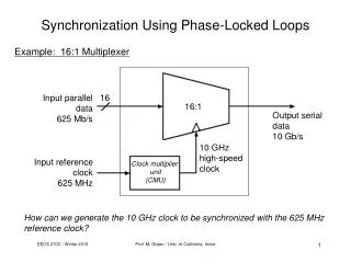
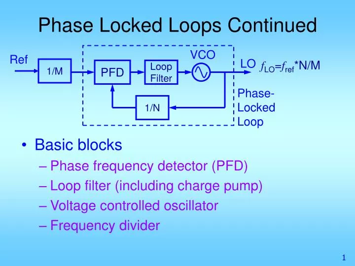
Phase Locked Loops Continued. Basic blocks Phase frequency detector (PFD) Loop filter (including charge pump) Voltage controlled oscillator Frequency divider. VCO. Ref. LO. f LO = f ref *N/M. 1/M. PFD. Loop Filter. Phase-Locked Loop. 1/N. Phase Locked Loops Continued. Key specs

E N D
Phase Locked Loops Continued • Basic blocks • Phase frequency detector (PFD) • Loop filter (including charge pump) • Voltage controlled oscillator • Frequency divider VCO Ref LO fLO=fref*N/M 1/M PFD Loop Filter Phase-Locked Loop 1/N
Phase Locked Loops Continued • Key specs • hold range: the frequency range over which phase tracking can be statically maintained • pull-in range: the frequency range over which PLL can become locked • pull-out range: dynamic limit of frequency range for stable operation • lock range: frequency range within which a PLL locks within one single-beat note between reference frequency and output frequency
Illustration of Static Ranges Very slowly vary input frequency
Phase Frequency Detector • Generates phase difference between the input signal and VCO output signal • Distinguish if VCO is faster or slower • Different types • Analog vs digital • Linear vs nonlinear
Analog phase detector: multiplier • Linear multiplier • Functions the same way as a mixer • But converting to DC (same frequencies) • Same mixer circuits can be used
2V, High-Frequency CMOS Multiplier • K-K Kan, D. Ma, K-C Mak and H.C. Luong, “Design Theory and Performance of a 1-GHz CMOS Downconversion and Upconversion Mixers,” Analog Integrated Circuit and Signal Processing, Vol. 24, No. 2, pp. 101-111, July 2000. • Based on the Gilbert cell • Can operate at a lower supply voltage because the mixer does not use stacking • • Source followers give better linearity • • Has a smaller mixer gain because sharing the bias currents with the followers • reduces gm
A Quarter-Square CMOS Multiplier • J.S. Pen˜a-Finol and J.A. Connelly, “A MOS Four-Quadrant Analog Multiplier Using the Quarter-Square Technique,” J. of Solid-State Circuits, vol. SC-22, No. 6, pp. 1064-1073, Dec. 1987.
CMOS Four-Quadrant Multiplier • Babanezhad and Temes - JSSC, Dec. 1985.
Digital phase-frequency detector • Compares edges of reference and divided clocks. • If reference clock leads the divided clock, the UP signal is asserted. • If the divided clock leads the reference clock , the DWN signal is asserted. • In an ideal PFD no pulses are present at the output in the locked state. • Duty cycle of inputs is not relevant to the circuit operation. • The width of the UP/DWN pulses is proportional to the phase difference between the clock inputs.
Digital phase-frequency detector • Conceptual diagram
Output of PFD for locked state • In locked state, narrow pulses are generated in both UP/DWN outputs. • The width of these pulses determines the amount of noise introduced to the VCO output by the charge-pump. • Timing mismatch between the UP/DWN pulses is a source of spurious tones.
The Charge-Pump converts the phase error information provided by the PFD into a voltage that controls the VCO frequency. • If UP is high, top switch is closed and charge is injected into capacitor, increasing voltage Vout • If DWN is high, bottom switch is closed and charge is extracted from capacitor,decreasing voltage Vout
State diagram Up=0; Dn=0; Up=0; Dn=1; Up=1; Dn=0;
Non-idealities • In practical PFD the delay of the gates creates non-idealities in the phase input/output characteristic. • The PFD can no longer resolve very small phase errors, and a dead zone is created. • To solve this problem, extra delay is introduced in the feedback path of reset signal.
Non-ideal effects of charge pumps • Current mismatch • Mismatch between source and sink currents in the charge pump introduces a finite phase error. • Current leakage • When the source/sink currents are off, leakage currents can flow and modify the VCO control voltage of the VCO by charging/discharging the loop filter. Spurs are introduced. • Charge sharing • Parasitic capacitances from the switches share charge with the loop filter when the nodes they are connected to have a large change in their voltage. • Charge injection • Occurs when switches are turned off and the charge in their channels is injected/extracted to the loop filter. Spurs are introduced
Precharge PFD • S. Kim, et. al., “A 960-Mb/s/pin Interface for Skew-Tolerant Bus Using Low Jitter PLL, IEEE J. of Solid-State Circuits, Vol. 32, No. 5, may 1997, pp. 691-700.
Modified Precharge PFD • H. O. Johansson, “A Simple Precharged CMOS Phase Fequency Detector,” IEEE J. of Solid-State Circuits, Vol. 33, No. 2, Feb. 1998, pp. 295-299.