Download

1 / 24
240 likes | 361 Views
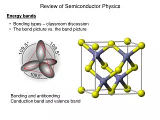
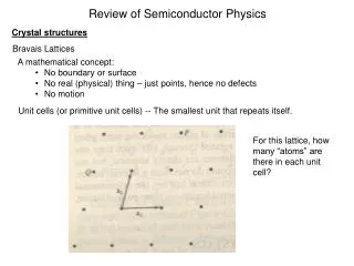
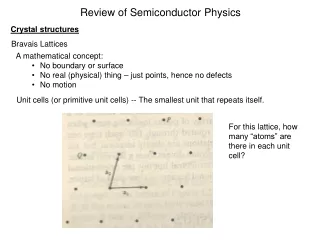
Review of Semiconductor Physics. Energy bands. Bonding types – classroom discussion The bond picture vs. the band picture. Bonding and antibonding Conduction band and valence band. The band gap is the consequence of Bragg diffraction: Two plane waves e ikx form standing waves

E N D
Review of Semiconductor Physics Energy bands • Bonding types – classroom discussion • The bond picture vs. the band picture Bonding and antibonding Conduction band and valence band
The band gap is the consequence of Bragg diffraction: Two plane waves eikx form standing waves - one peaks near the atoms and the other between them
Gap You can draw the E-k just in the 1st BZ.
The band picture – Bloch’s Theorem Notice it’s a theorem, not a law. Mathematically derived. The theorem: The eigenstates (r) of the one-electron Hamiltonian where V(r + R) = V(r) for all R in a Bravais lattice can be chosen to have the form of a plane wave times a function with the periodicity of the Bravais lattice: A periodic function u(r) is a solution, but the Bloch function is general. where un,k(r + R) = un,k(r) . Equivalently, Physical picture - Wave function
- Band structure Indirect gap 1D case 3D case 2/a 8/a a = 5.43 Å = 0.543 nm
Direct gap 2/a a = 5.65 Å = 0.565 nm 8/a
Limitations of the band theory Static lattice: Will introduce phonons Perfect lattice: Will introduce defects One-electron Shrödinger Eq: We in this class will live with this Justification: the effect of other electrons can be regarded as a kind of background.
Semi-classical theory Free electron Block electron ħkis the momentum. ħk is the crystal momentum, which is not a momentum, but is treated as momentum in the semiclassical theory. n is the band index. En(k) = En(k+K) 1D 3D 1D 3D un,k(r + R) = un,k(r) If you want to really understand the semiclassical theory and why you can treat the band edges as potentials, read (how?) James, Physical Review 76, 1611 (1949).
The Bloch (i.e. semiclassic) electron behaves as a particle following Newton’s laws. (We are back in the familiar territory.) • With a mass m* • Emerging from the other side of the first Brillouin zone upon hitting a boundary Newton’s 1st law: the Bloch electron moves forever Can get a current w/o applying a voltage? What is that constant speed if there’s no applied voltage (field/force)? Newton’s 2nd law: F = dp/dt = ħdk/dt Consider one electron, a full band of e’s, and a partial band of e’s Oscillation in dc field. So far not observed yet. Why?
Real crystals are not perfect. Defects scatter electrons. On average, the electron is scattered once every time period . Upon scattering, the electron forgets its previous velocity, and is “thermalized.” Mobility Note: It’s the defects, not the atoms (ions), that are scattering the electrons! How can we ignore the atoms (ions)?! The Drude (or crude?) model For a metal, you know n from its valence and atom density, so you know . = m / q The mean free path l = vth = vthm / q >> a
Values of k Discrete but quasi-continuous k = 2n/L, n = 1, 2, 3, …, N L = Na Run the (extra?) mile: Show the above by using the “periodic boundary” condition. Holes A vacancy in a band, i.e. a k-state missing the electron, behaves like a particle with charge +q. Run the (extra?) mile: Show the above.
Review of Semiconductor Physics Carrier Statistics • Fermi-Dirac distribution Nature prefers low energy. Lower energy states (levels) are filled first. Imagine filling a container w/ sands, or rice, or balls, or whatever • Each particle is “still” T = 0 K • Each has some energy, keeping bouncing around T > 0 K • Density of States How many states are there in the energy interval dE at E? D(E)dE 1D case derived in class. The take-home message: D(E) E1/2
2D case Run the extra mile Derive D(E) in 2D. Hint: count number of k’s in 2D. The answer: Or, for unit area D(E) = constant The take-home message: 3D case Run the extra mile Derive D(E) in 3D. Hint: count number of k’s in 2D. For unit area, The take-home message: D(E) E1/2
Things we have ignored so far: degeneracies Spin degeneracy: 2 Valley degeneracy: Mc Mc = 6 for Si
Total number of carriers per volume (carrier density, carrier concentration) Run the extra mile Derive the electron density n. Hint: Fermi-Dirac distribution approximated by Boltzmann distribution. Results for n and p are given. p is the total number of states NOT occupied. Doping One way to manipulate carrier density is doping. Doping shifts the Fermi level. np = ni2
One small thing to keep in mind: Subtle difference in jargons used by EEs and physicists We use the EE terminology, of course. Fermi level EF = EF(T) Same concept Physicists: (T) Chemical potential EF = (0) Fermi energy We already used for mobility.
Before we talk about devices, what are semiconductors anyway? Classroom discussion Na, K, … are metals Mg, Ca, … are also metals. Why? Si and Ge are semiconductors. Pb is a metal. Why can we modulate their properties by orders of magnitude? Classroom discussion Jezequel & Pollini, Phys Rev B 41, 1327 (1990)
We have mentioned defect scattering: Real crystals are not perfect. Defects scatter electrons. On average, the electron is scattered once every time period . Upon scattering, the electron forgets its previous velocity, and is “thermalized.” Mobility Any deviation from perfect periodicity is a defect. A perfect surface is a defect.
Phonons Static lattice approximation Atoms vibrate Harmonic approximation: springs Vibration quantized Each quantum is a phonon. Similar to the photon: E = ħ, p = ħk Phonons scatter carriers, too. The higher the temperature, the worse phonon scattering. You can use the temperature dependence of conductivity or mobility to determine the contributions of various scattering mechanisms.
Phonons = vk Sound wave in continuous media Microscopically, the solid is discrete. Phonon dispersion Wave vector folding, first Brillouin zone. Watch animation at http://en.wikipedia.org/wiki/File:Phonon_k_3k.gif Recall that Crystal structure = Bravais lattice + basis If there are more than 1 atom in the basis, optical phonons http://physics-animations.com/Physics/English/phon_txt.htm If you are serious and curious about photons, read Kittel, Introduction to Solid State Physics
Phonons in the 3D world -- Si In 3D, there are transverse and longitudinal waves. E = h = ħ 62 meV 15 THz When electron energy is low, the electron only interacts with acoustic phonons,
vd vsat E Optical phonons and transport At low fields, = 38 meV vth = 2.3 × 107 cm/s For Si, At high fields, vd comparable to vth Electrons get energy from the field, hotter than the lattice – hot electrons When the energy of hot electrons becomes comparable to that of optical phonons, energy is transferred to the lattice via optical phonons. Velocity saturation For Si, vsat ~ 107 cm/s
Alloys Compounds, alloys, heterostructures InP, GaAs, …, SiC InxGa1-xAsyP1-y, …, SixGe1-x Epitaxy Band structure of alloys
Topics • Review of Semiconductor physics • Crystal structure, band structures, band structure modification by alloys, heterostructurs, and strain • Carrier statistics • Scattering, defects, phonons, mobility, transport in heterostructures • Device concepts • MOSFETs, MESFETs, MODFETs, TFTs • Heterojunction bipolar transistors (HBT) • Semiconductor processing • Photodiodes, LEDs, semiconductor lasers • (optional) resonant tunneling devices, quantum interference devices, single electron transistors, quantum dot computing, ... • Introduction to nanoelectronics We will discuss heterostructures in the context of devices. More discussions on semiconductor physics will be embedded in the device context.