Download

1 / 28
350 likes | 806 Views
Semiconductor Device Physics. Lecture 2 Dr. Gaurav Trivedi , EEE Department, IIT Guwahati. Electronic Properties of Si. Silicon is a semiconductor material. Pure Si has a relatively high electrical resistivity at room temperature. Th ere are 2 types of mobile charge-carriers in Si:

E N D
Semiconductor Device Physics Lecture 2 Dr. GauravTrivedi, EEE Department, IIT Guwahati
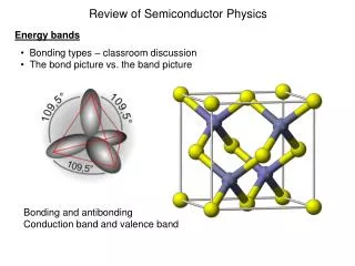
Electronic Properties of Si • Silicon is a semiconductor material. • Pure Si has a relatively high electrical resistivity at room temperature. • There are 2 types of mobile charge-carriers in Si: • Conduction electrons are negatively charged, e=–1.602 10–19 C • Holes are positively charged, p=+1.602 10–19C • The concentration (number of atom/cm3) of conduction electrons & holes in a semiconductor can be influenced in several ways: • Adding special impurity atoms (dopants) • Applying an electric field • Changing the temperature • Irradiation
Si Si Si Si Si Si Si Si Si Bond Model of Electrons and Holes • 2-D Representation Hole • When an electron breaks loose and becomes a conduction electron, then a hole is created. Conductionelectron
What is a Hole? • A hole is a positive charge associated with a half-filled covalent bond. • A hole is treated as a positively charged mobile particle in the semiconductor.
Conduction Electron and Hole of Pure Si • Covalent (shared e–) bonds exists between Si atoms in a crystal. • Since the e– are loosely bound, some will be free at any T, creating hole-electron pairs. ni≈ 1010 cm–3 at room temperature ni= intrinsic carrier concentration
Si: From Atom to Crystal Energy states (in Si atom) Energy bands (in Si crystal) • The highest mostly-filled band is the valence band. • The lowest mostly-empty band is the conduction band.
Energy Band Diagram Ec EG, band gap energy Electron energy Ev • For Silicon at 300 K, EG = 1.12 eV • 1 eV = 1.6 x 10⁻¹⁹ J • Simplified version of energy band model, indicating: • Lowest possible conduction band energy (Ec) • Highest possible valence band energy (Ev) • Ec and Ev are separated by the band gap energy EG.
Measuring Band Gap Energy • EGcan be determined from the minimum energy (hn) of photons that can be absorbed by the semiconductor. • This amount of energy equals the energy required to move a single electron from valence band to conduction band. Electron Ec Photon photon energy: hn= EG Ev Hole Band gap energies
Carriers • Completely filled or empty bands do not allow current flow, because no carriers available. • Broken covalent bonds produce carriers (electrons and holes) and make current flow possible. • The excited electron moves from valence band to conduction band. • Conduction band is not completely empty anymore. • Valence band is not completely filled anymore.
E v E c Band Gap and Material Classification E c = E ~8 eV G E c = E 1.12 eV E G c E E E v v v Metal Si SiO2 • Insulators have large band gap EG. • Semiconductors have relatively small band gap EG. • Metals have very narrow band gap EG . • Even, in some casesconduction band is partially filled,Ev> Ec.
Carrier Numbers in Intrinsic Material • More new notations are presented now: • n : number of electrons/cm3 • p : number of holes/cm3 • ni: intrinsic carrier concentration • In a pure semiconductor, n = p = ni. • At room temperature, • ni= 2 106 /cm3 in GaAsni= 1 1010 /cm3 in Si ni= 2 1013 /cm3 in Ge
Donors: P, As, Sb Acceptors: B, Ga, In, Al Manipulation of Carrier Numbers – Doping • By substituting a Si atom with a special impurity atom (elements from Group IIIorGroup V), a hole or conduction electron can be created.
Doping Silicon with Acceptors • Example: Aluminium atom is doped into the Si crystal. Al– is immobile • The Al atom accepts an electron from a neighboring Si atom, resulting in a missing bonding electron, or “hole”. • The hole is free to roam around the Si lattice, and as a moving positive charge, the hole carries current.
Doping Silicon with Donors • Example: Phosphor atom is doped into the Si crystal. P+ is immobile • The loosely bounded fifth valence electron of the P atom can “break free” easily and becomes a mobile conducting electron. • This electron contributes in current conduction.
E c ED Donor Level Donor ionization energy Acceptor ionization energy Acceptor Level E A E v Donor / Acceptor Levels (Band Model) ▬ + ▬ + Ionization energy of selected donors and acceptors in Silicon Donors Acceptors Sb P As B Al In Ionization energy of dopant EC – ED or EA – EV(meV) 39 45 54 45 67 160
Dopant Ionization (Band Model) • Donor atoms • Acceptor atoms
Carrier-Related Terminology • Donor: impurity atom that increases n (conducting electron).Acceptor: impurity atom that increases p (hole). • n-type material: contains more electrons than holes.p-type material: contains more holes than electrons. • Majority carrier: the most abundant carrier.Minority carrier: the least abundant carrier. • Intrinsic semiconductor: undoped semiconductor n = p = ni.Extrinsic semiconductor: doped semiconductor.
DE Ec Ev Density of States E gc(E) Ec density of states g(E) Ev gv(E) • g(E) is the number of states per cm3 per eV. • g(E)dE is the number of states per cm3 in the energy range between E and E+dE).
DE Ec Ev Density of States E gc(E) Ec density of states g(E) Ev gv(E) • Near the band edges: E Ec EEv mo: electron rest mass
Fermi Function • The probability that an available state at an energy E will be occupied by an electron is specified by the following probability distribution function: k : Boltzmann constant T : temperature in Kelvin • EF is called the Fermi energy or the Fermi level.
Equilibrium Distribution of Carriers • n(E) is obtained by multiplying gc(E) and f(E),p(E) is obtained by multiplying gv(E) and 1–f(E). • Intrinsic semiconductor material Energy band diagram Density of states Carrier distribution Probability of occupancy
Equilibrium Distribution of Carriers • n-type semiconductor material Energy band diagram Density of States Carrier distribution Probability of occupancy
Equilibrium Distribution of Carriers • p-type semiconductor material Energy band diagram Density of States Carrier distribution Probability of occupancy
Important Constants • Electronic charge, q = 1.610–19 C • Permittivity of free space, εo = 8.85410–12 F/m • Boltzmann constant, k = 8.6210–5eV/K • Planck constant, h = 4.1410–15eVs • Free electron mass, mo = 9.110–31 kg • Thermal energy, kT = 0.02586 eV (at 300 K) • Thermal voltage,kT/q = 0.02586 V (at 300 K)