Download

1 / 70
920 likes | 1.62k Views
Physics of semiconductor devices. Nihar R. Mahapatra. Bonding in solids. The interaction of electrons in neighboring atoms of a solid serves the very important function of holding the crystal together. For example Nacl

E N D
Physics of semiconductor devices Nihar R. Mahapatra
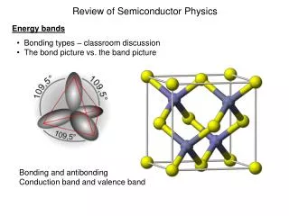
Bonding in solids The interaction of electrons in neighboring atoms of a solid serves the very important function of holding the crystal together.
For example Nacl In the Nacl lattice, each Na atom is surrounded by 6 nearest neighbor Cl atoms and vice versa. The electronic structure of Na ( Z=11) is [Ne] 3S1, Cl ( z=17) has the structure [Ne] 3S2 3P5. In the lattice each Na atom gives up its outer 3S electron to a Cl atom, so that the crystal is made up of ions with the electronic structure of the inert atoms Ne & Ar ([Ne] 3S23P6). However, the ions have net electric charges after the electron exchange. The Na+ ion has a net +ve charge, having lost an electron, and the Cl- ion has a net –ve charge, having gained an electron. Each Na+ ion exerts an electrostatic attractive force upon its ‘6’ Cl- neighbors and vice versa. These columbic forces pull the lattice together until a balance is reached with repulsive forces. An important observation in the Nacl structure is that all electrons are tightly bound to atoms. Once the electron exchanges have been made between the Na & Cl atoms to form the Na+ and Cl- ions, the outer orbits of all atoms are completely filled. Since the ions have the closed shell configuration of the inert atoms Ne & Ar, there are no loosely bound electrons to participate in current flow; as a result Nacl is a good insulator.
In a metal atom the outer electronic shell is only partially filled, usually by no more than ‘3’ electrons. For example the alkali metal ( Na) have only one electron in the outer orbit. This electron is loosely bound and is given up easily in ion formation. This accounts for the great chemical activity in the alkali metals as well as for their high electrical conductivity. In the metal the outer electron of each alkali atom is contributed to the crystal as a whole, so that the solid is made up of ions with closed shells immersed in a sea of free electrons. The forces holding the lattice together arise from an interaction between the +ve ion cores and the surrounding free electrons. This is metallic bonding. The metals have the sea of electrons and these electrons are free to move about the crystal under the influence of an electric field. A third type of bonding is exhibited by the diamond lattice semiconductors. Each atom in the Ge, Si or C diamond lattice is surrounded by four nearest neighbors, each with ‘4’ neighbors. The bonding forces arise from a quantum mechanical interaction between the shared electrons. This is known as covalent bonding. As in the case of the ionic crystals, no free electrons are available to the lattice in the covalent diamond structure. By this reasoning Ge & Si should also be insulators. But we shall see an electron can be thermally or optically excited out of a covalent bond and thereby become free to participate in conduction. This is an important feature of semiconductors.
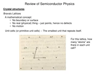
As isolated atoms are brought together to form a solid, various interactions occur between neighboring atoms. The forces of attraction and repulsion between atoms will find a balance at the proper inter-atomic spacing for the crystal. In the process, important changes occur in the electron energy level configurations and these changes result in the varied electrical properties of solids. Si14:-1s2 2s2 2p6 3s2 3p2
In the outermost shell or valence shell, n=3, two 3s and two 3p electrons interact to form the four ‘hybridized’ sp3 electrons when the atoms are brought close together. Solving the Schrödinger equation for such an interacting system, the composite two electron wave functions are linear combinations of the individual atomic orbital (LCAO). When the atoms are brought together, the application of the Pauli Exclusion Principle becomes important. When two atoms are completely isolated from each other so that there is no interaction of electron wave functions between them, they can have identical electronic structures. As the spacing between the two atoms becomes smaller, electron wave functions begin to overlap. The exclusion principle says that no two electrons in a given interacting system may have the same quantum state. Thus there must be at most one electron per level after there is a splitting of the discrete energy levels of the isolated atoms into new levels belonging to the pair rather than to individual atoms.
In a solid, many atoms are brought together so that the split energy levels form continuous bands of energies. Each isolated silicon atom has an electronic structure 1s2 2s2 2p6 3s2 3p2 in the ground state. If we consider N atoms, there will be 2N, 2N, 6N, 2N and 6N states of type 1s, 2s, 2p, 3s, 3p respectively. As the inter-atomic space decreases, these energy levels split into bands, beginning with the outer (n=3) shell. The 3s and 3p bands merge into a single band composed of a mixture of energy levels. This band of 3s-3p levels contains 8N available states. As the distance between atoms approaches the equilibrium inter-atomic spacing of silicon, this band splits into two bands separated by an energy gap Eg. The upper band called the conduction band contains 4N states, as does the lower band called the valence band. Thus apart from the low lying and tightly bound core levels, the silicon crystal has two bands of available energy levels separated by an energy gap Eg which contains no allowed energy levels for electrons to occupy. This gap is sometimes called a ‘forbidden band’, since in a perfect crystal it contains no electron energy states. The lower 1s band is filled with the 2N electrons. 2s and 2p bands will have 2N and 6N electrons in them respectively. However, there are 4N electrons in the original isolated (n=3) shells (2N in 3s states and 2N in 3p states). These 4N electrons must occupy states in the valence band or the conduction band in the crystal. At 0K, the electrons will occupy the lowest energy states available to them. In the case of the Si crystal, there are exactly 4N states in the valence band available to the 4N electrons. Thus at 0K, every state in the valence band will be filled, while the conduction band will be completely empty of electrons.
If we apply an electric field to the free electron and use Newton’s classical equation of motion. Consider the allowed energy band in the figure. The energy near the bottom of this energy band may be approximated by a parabola just as that of a free particle. The energy is the energy at the bottom of the band. Since, is a positive quantity.
Insulators, Semiconductors, Metals • The last completely filled (at least at T = 0 K) band is called the Valence Band • The next band with higher energy is the Conduction Band • The Conduction Band can be empty or partially filed • The energy difference between the bottom of the CB and the top of the VB is called the Band Gap (or Forbidden Gap)
Consider a solid with the empty Conduction Band If apply electric field to this solid, the electrons in the valence band (VB) cannot participate in transport (no current) Insulators, Semiconductors, Metals
Insulators, Semiconductors, Metals • The electrons in the VB do not participate in the current, since • Classically, electrons in the electric field accelerate, so they acquire [kinetic] energy • In QM this means they must acquire slightly higher energy and jump to another quantum state • Such states must be available, i.e. empty allowed states • But no such state are available in the VB! This solid would behave as an insulator
Consider a solid with the half filled Conduction Band (T = 0K) If an electric field is applied to this solid, electrons in the CB do participate in transport, since there are plenty of empty allowed states with energies just above the Fermi energy This solid would behave as a conductor (metal) Insulators, Semiconductors, Metals
Band Overlap • Many materials are conductors (metals) due to the “band overlap” phenomenon • Often the higher energy bands become so wide that they overlap with the lower bands • additional electron energy levels are then available
Band Overlap • Example: Magnesium (Mg; Z =12): 1s22s22p63s2 • Might expect to be insulator; however, it is a metal • 3s-band overlaps the 3p-band, so now the conduction band contains 8N energy levels, while only have 2N electrons • Other examples: Zn, Be, Ca, Bi
Band Hybridization • In some cases the opposite occurs • Due to the overlap, electrons from different shells form hybrid bands, which can be separated in energy • Depending on the magnitude of the gap, solids can be insulators (Diamond); semiconductors (Si, Ge, Sn; metals (Pb)
Insulators, Semiconductors, Metals • There is a qualitative difference between metalsandinsulators(semiconductors) • the highest energy band “containing” electrons is only partially filled for Metals (sometimes due to the overlap) • Thus they are good conductors even at very low temperatures • The resisitvity arises from the electron scattering from lattice vibrations and lattice defects • Vibrations increases with temperature higher resistivity • The concentration of carriers does not change appreciably with temperature
Insulators, Semiconductors, Metals • The difference betweenInsulatorsandSemiconductorsis “quantitative” • The difference in the magnitude of the band gap • Semiconductors are “Insulators” with a relatively small band gap • At high enough temperatures a fraction of electrons can be found in the conduction band and therefore participate in transport
Insulators vs Semiconductors • There is no difference between Insulatorsand Semiconductors at very low temperatures • In neither material are there any electrons in the conduction band – and so conductivity vanishes in the low temperature limit
Insulators vs Semiconductors • Differences arises at high temperatures • A small fraction of the electrons is thermally excited into the conduction band. These electrons carry current just as in metals • The smaller the gap the more electrons in the conduction band at a given temperature • Resistivity decreases with temperature due to higher concentration of electrons in the conduction band
Conduction Electrical current for holes and electrons in the same direction
4 4 Conduction band Conduction band GaAs Si 3 3 2 2 ΔE=0.31 Energy (eV) 1 Energy (eV) 1 Eg Eg 0 0 -1 -1 Valance band Valance band -2 -2 k [111] 0 [100] k [111] 0 [100] Energy band structures of GaAs and Si
4 Conduction band Band gap is the smallest energy separation between the valence and conduction band edges. GaAs 3 2 ΔE=0.31 Energy (eV) 1 The smallest energy difference occurs at the same momentum value Eg 0 -1 Valance band Direct band gap semiconductor -2 k [111] 0 [100] Energy band structure of GaAs
4 The smallest energy gap is between the top of the VB at k=0 and one of the CB minima away from k=0 Conduction band Si 3 2 Energy (eV) Indirect band gap semiconductor 1 Eg 0 • Band structure of AlGaAs? • Effective masses of CB satellites? • Heavy- and light-hole masses in VB? -1 Valance band -2 k [111] 0 [100] Energy band structure of Si
E E E direct transition Eg k
E E Eg direct transition k
E Eg k
E Eg indirect transition k
E Eg indirect transition k
The Semiconductor in Equilibrium (A key chapter in this course) • Derive the thermal-equilibrium concentrations of electrons and holes in a semiconductor as a function of the Fermi energy level. • Discuss the process by which the properties of a semiconductor material can be favorably altered by adding specific impurity atoms to the semiconductor. • Determine the thermal-equilibrium concentrations of electrons and holes in a semiconductor as a function of the concentration of dopant atoms added to the semiconductor. • Determine the position of the Fermi energy level as a function of the concentrations of dopant atoms added to the semiconductor.
4.1 | CHARGE CARRIERS IN SEMICONDUCTORS 4.1.1 Equilibrium Distribution of Electrons and Holes • a plot of the density of states function in the conduction-band gc(E), the density of states function in the valence-band gv(E), and the Fermi–Dirac probability function for T > 0 K when EF is approximately halfway between Ecand Ev. • Assume that the electron and hole effective masses are equal, then gc(E) and gv(E) are symmetrical functions about the midgapenergy. • Note that the function fF (E ) for E > EF is symmetrical to the function 1 - fF (E) for E < EF about the energy E = EF.
4.1.2 The n0 and p0 Equations Thermal-Equilibrium Electron Concentration
Comment of Example 4.1: The probability of a state being occupied can be quite small, but the fact that there are a large number of states means that the electron concentration is a reasonable value.
Comment of Ex 4.2: The parameter values at any temperature can easily be found by using the 300 K values and the temperature dependence. Note that the value of Nc for gallium arsenide is smaller than the typical 1019 cm-3 value due to the small electron effective mass in gallium arsenide.
Comment of Ex 4.3: the intrinsic carrier concentration increased by over 4 orders of magnitude as the temperature increased by 150°C. • the value of ni for these semiconductors may easily vary over several orders of magnitude as the temperature changes over a reasonable range.
4.1.4 The Intrinsic Fermi-Level Position The intrinsic Fermi level must shift away from the band with the larger density of states in order to maintain equal numbers of electrons and holes.