Download
1 / 36
370 likes | 397 Views
Explore microoperations on shift registers, including parallel loading, bi-directional operations, and counters, with detailed explanations and examples. Learn how to control shifts and loads effectively.

E N D
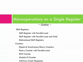
Microoperations on a Single Register ~ Outline ~ Shift Registers Shift Register with Parallel Load Shift Register with Parallel Load and Hold Bidirectional Shift Registers Counters Ripple & Synchronous Binary Counters Binary Counter with Parallel Load BCD Counter Modulo-N Counter Arbitrary Count Sequence
Shift Registers move data laterally within the register toward its MSB or LSB position In the simplest case, the shift register is simply a set of D flip-flops connected in a row like this: Shift Registers *CP: a common clock pulse input that activates the shift
Data input, In, is called a serial inputor the shift right input. Data output, Out, is often called the serial output. The vector (A, B, C, Out) is called the parallel output. Shift Registers Parallel Output Serial Output Serial Input
Shift Registers • T0 is the register state just before the first clock pulse occurs • T1 is after the first pulse and before the second. • Initially unknown states are denoted by “x” • Complete the last three rows of the table
Shift Registers with Parallel Load • The shift register shown earlier has no control input, thus data is always shifted on clock pulse. • How to make the shift registers more controllable? • E.g. shifts only on select positive clock edges. • Shift operation can be controlled through D inputs of the FFs, rather than through the clock inputs CP.
By adding a mux between each shift register stage, data can be shifted or loaded If SHIFT is LOW, A and B are replaced by the data on DA and DB lines, else data shifts right on each clock. Shift Registers with Parallel Load Serial Input 2-to-1 MUX Dn A0 A1 IN Selector SHIFT
Shift Registers with Parallel Loads and Hold • But what if we want to hold to the current data, meaning no shift or no loading of new data? • The design must have 2 controls: • For the SHIFT • For the LOAD Function Table for the Register of Fig 7-10 We use an AND gate to disabled the Load input, so we mark with don’t care condition
4-bit SHIFT REGISTER WITH PARALLEL LOAD AND HOLD OPERATION In Register Transfer Language: Control inputs AND gates: S: Enables the Shift operation D: Enables the input data Q: Restores the contents of reg. when no operation Shift : Q sl Q, Shift Load : Q D S S S S D D D D Q Q Q Q Figure 7-10 M. Morris Mano LOGIC AND COMPUTER DESIGN FUNDAMENTALS
Shift Registers with Parallel Loads and Hold Shift : Q sl Q, Shift Load : Q D S • S = 0, L = 0 : • AND3 (Q) in each stage is enabled • The output of each FF is applied to its own D input. • A +ve transition of CLK restores the contents of reg. • Output Qi is unchanged D Q
Shift Registers with Parallel Loads and Hold Shift : Q sl Q, Shift Load : Q D S • S = 0, L = 1 : • AND2 (D) in each stage is enabled • The input Di is applied to D input of corresponding FF. • Next +ve transition of CLK transfers the parallel input data into reg. • Output Qi = Di D Q
Shift Registers with Parallel Loads and Hold Shift : Q sl Q, Shift Load : Q D S • S = 1 : • AND1 (S) in each stage is enabled When +ve edge occurs on CLK: • Data from serial input SI to be transferred to FF Q0, • Output Q0 to be transferred to FF Q1, …and so on down the line. D Q
Bidirectional Shift Register • Unidirectional Register • Capable of shifting in only one direction (like what we have discussed in previous lectures) • Shift on clock pulse • Shift & Load • Shift, Load & Hold * shift occurs in one direction only • Bidirectional Register • A register that can shift in both directions • Shift Left (sl) • Shift Right (sr) And at the same time is capable of HOLD and LOAD
A0 A1 A2 A3 4-to -1 MUX S0 S1 Bidirectional Shift Register • By placing a 4-input multiplexer in front of each D flip-flop in a shift register, we can implement a circuit with shift right, shift left, parallel load, hold. • Each stage consists of a D-FF and 4:1 multiplexer 0 1 2 3 D
Bidirectional Shift Register How do we represent this in RTL?? S1S0 : Q Q (No Transfer occurs) S1S0 : Q sl Q S1S0 : Q sr Q S1S0 : Q D
Bidirectional Shift Register Let’s analyze the one stage diagram of a Bidirectional Shift Register with parallel load.
LSB 7 6 5 4 3 2 1 0 4-Bit Bidirectional Shift Register with Parallel Load Serial outputs: (Right Shift) (Left Shift) MSB sr sl LSI RSI
Bidirectional Shift Register • Shift registers can also be designed to shift more than a single bit position right or left • Shift register can be designed to shift a variable number of bit positions specified by a variable called a shift amount.
Counter • A register that goes through a prescribed sequence of distinct states upon the application of a sequence of input pulses. • Input pulses may be clock pulses or from other source, may occur at regular or irregular intervals of time. • Binary counter: • a counter that follows the binary number sequence. • An n-bit binary counter consists of n FFs • Can count in binary from 0 through 2 -1 • Counter are available in two categories; i.e. ripple counters and synchronous counters n
Ripple Counter • A positive edge to the C input of each FFs causes the FF to complement its state. • The complemented output of each FF is connected to the C input of the next most significant FF. • The FF holding the least significant bit (Q0) receives the incoming clock pulses. • The C inputs of some FFs are triggered not by the common clock pulse, but rather by the transitions that occur in other FF outputs.
Ripple Counter • Advantage: the simple hardware • Disadvantage: • asynchronous circuits, • With added logics, can become circuits with delay dependence • unreliable operation
Synchronous Counter • The clock pulse applied to the C inputs of ALL FFs • The clock pulse triggers all FFs simultaneously • To eliminate the "ripple" effects • The carry output CO is used to extend the counter to more stages Serial Gating
Synchronous Counter • For an up-counter (counts up by 1), an incrementer and D-FF can be used.
Synchronous Counter • Internal Logic • XOR complements each bit • AND chain causes complement of a bit if all bits toward LSB from it equal 1 • Count Enable • Forces all outputs of AND chain to 0 to “hold” the state • Carry Out • Added as part of incrementer • Connect to Count Enable of additional 4-bit counters to form larger counters Serial Gating
Binary Counter with Parallel Load • Add path for input data, Di • enabled for Load = 1 • Add logic to: • Disable count logic for Load = 1 • Disable feedback from outputs for Load = 1 • Enable count logic for Load = 0 & Count = 1 • The resulting function table:
Load 4-bit Binary Counter with Parallel Load Count Carry Output, CO Clock
Converting parallel load counter into synchronous BCD counter • Connect an external AND gate to Load • Counter starts with all-zero output (0000) • Count input always HIGH (1)
Converting parallel load counter into synchronous BCD counter • AND gate = 0 (LOAD = 0), BCD counts from 0000 to 1001 • Output = 1001, Q0 and Q3 in HIGH, AND gate = 1 (LOAD = 1) • Next clock transition, counter load inputs (D0 D3) = 0000 following 1001 into counter. 1 0 1 1 1 0 0 0 0 0 1 0
Converting parallel load counter into synchronous BCD counter Y
Synchronous BCD Counter • Y = 1, when present state = 1001 • Y = Q1Q8 • FF input equations: • Simplify using K – map • Obtained from next – state values • 1010 ~ 1111 don’t care (X)
Modulo – N Counter • A counter that goes through a repeated sequence of N states • Maximum decimal number to be counted : • If Mod N = 2n then the max decimal counted is N-1 • If Mod 16, then the max decimal number is 15 • To determine the required number of flip-flops: • n flip-flop 2n output = Mod N
Modulo – 7 Counter • Use a synchronous 4 – bit binary counter with a synchronous LOAD and C • LOAD – detect count “6” and load “0” • Gives count of (0, 1, 2, 3, 4, 5, 6, 0, 1, …) – 7 states • Using don’t care for states above 0110 • Detect number “6” when LOAD = Q2Q1 (0110) • Next clock transition, counter load inputs (D0 D3) = 0000 following 0110 into counter. 1 0 0 0 0 0 1 1 0 0 0 0 0 1
Modulo – 6 Counter : Special requirement Requirement: Synchronously preset “9” on RESET and LOAD “9” on terminal count “14” 1 1 1 • Use a synchronous 4 – bit binary counter with a synchronous LOAD • Use LOAD signal to : • preset count to “9” • detect count “14” • Gives count of (9, 10, 11, 12, 13, 14, 9, 10, …) – 6 states • Next clock transition, counter load inputs (D0 D3) = 1001 following 1110 into counter. 1 0 1 0 0 1 1 1
Arbitrary Count Sequence • Design a counter with sequence of six states as in Table 7-10 2 states are not included in this table: 011 and 111
Arbitrary Count Sequence • Simplified equations :
Arbitrary Count Sequence • Logic diagram of the arbitrary counter: