Download
1 / 97
990 likes | 1.08k Views
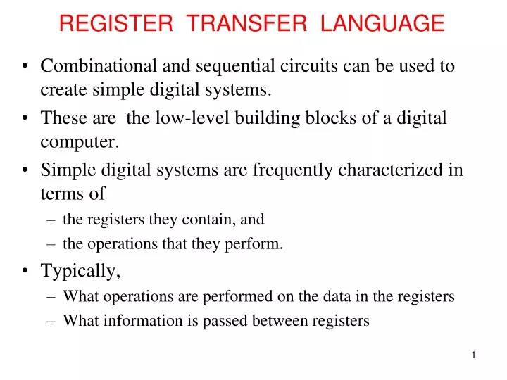
REGISTER TRANSFER LANGUAGE. Combinational and sequential circuits can be used to create simple digital systems. These are the low-level building blocks of a digital computer. Simple digital systems are frequently characterized in terms of the registers they contain, and

E N D
REGISTER TRANSFER LANGUAGE • Combinational and sequential circuits can be used to create simple digital systems. • These are the low-level building blocks of a digital computer. • Simple digital systems are frequently characterized in terms of • the registers they contain, and • the operations that they perform. • Typically, • What operations are performed on the data in the registers • What information is passed between registers
MICROOPERATIONS (1) • The operations executed on data stored in registers are called microoperations. • Examples of microoperations • Shift • Load • Clear • Increment • Count
INTERNAL HARDWARE ORGANIZATION OF A DIGITAL SYSTEM • Definition of the internal hardware organization of a computer - Set of registers it contains and their function - The sequence of microoperations performed on the binary information stored in the registers - Control signals that initiate the sequence of microoperations (to perform the functions)
REGISTER TRANSFER LANGUAGE • The symbolic notation used to describe the microoperation transfers among registers is called a Register transfer language. • Register transfer language • A symbolic language • A convenient tool for describing the internal organization of digital computers • Can also be used to facilitate the design process of digital systems.
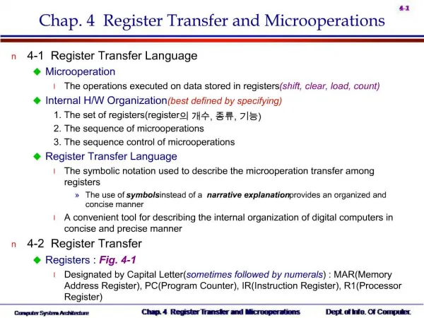
Register Transfer • Registers are designated by capital letters, sometimes followed by numbers (e.g., A, R13, IR). • Often the names indicate function: MAR - memory address register PC - program counter IR - instruction register • Information transfer from one register to another is designated in symbolic form by means of a replacement operator. R2 R1 • In this case the contents of register R1 are copied (loaded) into register R2 and contents of R1 remains same.
Block diagram of a register 7 6 5 4 3 2 1 0 R1 Register R Showing individual bits 15 0 15 8 7 0 PC(H) R2 PC(L) Numbering of bits Subfields (Divided into two parts)
Often we want the transfer to occur only under a predetermined control condition. if (p=1) then (R2 R1) where ‘p’ is a control signal generated in the control section. • In digital systems, this is often done via a control signal, called a control function • If the signal is 1, the action takes place • This is represented as: P: R2 R1
HARDWARE IMPLEMENTATION OF CONTROLLED TRANSFERS Implementation of controlled transfer P: R2 R1 Load P Control Circuit Block diagram R2 Clock n R1 t t+1 Timing diagram Clock Load Transfer occurs here • The same clock controls the circuits that generate the control function and the destination register • Registers are assumed to use positive-edge-triggered flip-flops
SIMULTANEOUS OPERATIONS • If two or more operations are to occur simultaneously, they are separated with commas P: R3 R5, MAR IR • Here, if the control function P = 1, load the contents of R5 into R3, and at the same time (clock), load the contents of register IR into register MAR
BASIC SYMBOLS FOR REGISTER TRANSFERS Symbols Description Examples Capital letters Denotes a register MAR, R2 & numerals Parentheses () Denotes a part of a register R2(0-7), R2(L) Arrow Denotes transfer of information R2 R1 Colon : Denotes termination of control function P: Comma , Separates two micro-operations A B, B A
Bus and Memory Transfers Register A Register B Register C Register D Bus lines Register A Register B Register C Register D 1 2 3 4 1 2 3 4 1 2 3 4 1 2 3 4 B C D B C D B C D B C D 1 1 1 2 2 2 3 3 3 4 4 4 0 0 0 0 4 x1 4 x1 4 x1 4 x1 MUX MUX MUX MUX x select y 4-line bus BUS AND MEMORY TRANSFERS Bus is a path(of a group of wires) over which information is transferred, from any of several sources to any of several destinations. From a register to bus: BUS R
Bus and Memory Transfers TRANSFER FROM BUS TO A REGISTER Bus lines Load Reg. R0 Reg. R1 Reg. R2 Reg. R3 D D D D 0 1 2 3 z E (enable) Select 2 x 4 w Decoder Three-State Bus Buffers Output Y=A if C=1 High-impedence if C=0 Normal input A Control input C Bus line with three-state buffers Bus line for bit 0 A0 B0 C0 D0 0 S0 Select 1 S1 2 Enable 3
Bus and Memory Transfers BUS TRANSFER IN RTL • Depending on whether the bus is to be mentioned explicitly or not, register transfer can be indicated as either or • In the former case the bus is implicit, but in the latter, it is explicitly indicated R2 R1 BUS R1, R2 BUS
Bus and Memory Transfers data input lines n address lines k RAM unit Read Write n data output lines MEMORY (RAM) • Memory (RAM) can be thought as a sequential circuits containing some number of registers • These registers hold the words of memory • Each of the r registers is indicated by an address • These addresses range from 0 to r-1 • Each register (word) can hold n bits of data • Assume the RAM contains r = 2k words. It needs the following • n data input lines • n data output lines • k address lines • A Read control line • A Write control line
Bus and Memory Transfers Read Memory unit AR Write Data out Data in MEMORY TRANSFER • Collectively, the memory is viewed at the register level as a device, M. • Since it contains multiple locations, we must specify which address in memory we will be using • This is done by indexing memory references • Memory is usually accessed in computer systems by putting the desired address in a special register, the Memory Address Register (MAR, or AR) • When memory is accessed, the contents of the MAR get sent to the memory unit’s address lines M
Bus and Memory Transfers MEMORY READ • To read a value from a location in memory and load it into a register, the register transfer language notation looks like this: • This causes the following to occur • The contents of the MAR get sent to the memory address lines • A Read (= 1) gets sent to the memory unit • The contents of the specified address are put on the memory’s output data lines • These get sent over the bus to be loaded into register R1 R1 M[MAR]
Bus and Memory Transfers MEMORY WRITE • To write a value from a register to a location in memory looks like this in register transfer language: • This causes the following to occur • The contents of the MAR get sent to the memory address lines • A Write (= 1) gets sent to the memory unit • The values in register R1 get sent over the bus to the data input lines of the memory • The values get loaded into the specified address in the memory M[MAR] R1
Bus and Memory Transfers SUMMARY OF R. TRANSFER MICROOPERATIONS A B Transfer content of reg. B into reg. A AR DR(AD) Transfer content of AD portion of reg. DR into reg. AR A constant Transfer a binary constant into reg. A ABUS R1, Transfer content of R1 into bus A and, at the same time, R2 ABUS Transfer content of bus A into R2 AR Address register DR Data register M[R] Memory word specified by reg. R M Equivalent to M[AR] DR M Memory read operation: transfers content of memory word specified by AR into DR M DR Memory write operation: transfers content of DR into memory word specified by AR
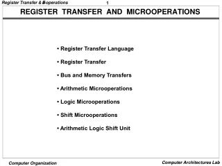
ARITHMETIC MICROOPERATIONS Computer system microoperations are of four types: 1. Register transfer microoperations transfer binary information from one register to another 2. Arithmetic microoperations perform arithmetic operations on numeric data stored in registers. 3.Logic microoperationsperform bit manipulation operations on non numeric data stored in registers. 4.Shift microoperationsperform shift operations on data stored in registers.
ARITHMETIC MICROOPERATIONS • The basic arithmetic microoperations are • Addition • Subtraction • Increment • Decrement • The additional arithmetic microoperations are • Add with carry • Subtract with borrow • Transfer/Load • etc. … Table: Arithmetic Micro-Operations R3 R1 + R2 Contents of R1 plus R2 transferred to R3 R3 R1 - R2 Contents of R1 minus R2 transferred to R3 R2 R2’ Complement the contents of R2 R2 R2’+ 1 2's complement the contents of R2 (negate) R3 R1 + R2’+ 1 subtraction R1 R1 + 1 Increment R1 R1 - 1 Decrement
BINARY ADDER / SUBTRACTOR / INCREMENTER Binary Adder Binary Adder-Subtractor Binary Incrementer
ARITHMETIC CIRCUIT Cin S1 S0 A0 X0 C0 D0 S1 FA S0 Y0 C1 4x1 B0 0 1 MUX 2 3 A1 X1 C1 D1 S1 FA S0 Y1 C2 B1 4x1 0 1 MUX 2 3 A2 X2 C2 S1 D2 FA S0 Y2 C3 4x1 B2 0 1 MUX 2 3 A3 X3 C3 D3 S1 FA S0 Y3 C4 4x1 B3 0 1 MUX 2 Cout 3 0 1 S1 S0 Cin Y Output Microoperation 0 0 0 B D = A + B Add 0 0 1 B D = A + B + 1 Add with carry 0 1 0 B’ D = A + B’ Subtract with borrow 0 1 1 B’ D = A + B’+ 1 Subtract 1 0 0 0 D = A Transfer A 1 0 1 0 D = A + 1 Increment A 1 1 0 1 D = A - 1 Decrement A 1 1 1 1 D = A Transfer A
A B F0 F1 F2 … F13 F14 F15 0 0 0 0 0 … 1 1 1 0 1 0 0 0 … 1 1 1 1 0 0 0 1 … 0 1 1 1 1 0 1 0 … 1 0 1 LOGIC MICROOPERATIONS • It specifies binary operations on the strings of bits stored in registers • Logic microoperations are bit-wise operations, i.e., they work on the individual bits of data • useful for bit manipulations on binary data • useful for making logical decisions based on the bit value • There are, in principle, 16 different logic functions that can be defined over two binary input variables • However, most systems only implement four of these • AND (), OR (), XOR (), Complement/NOT • The others can be created from combination of these
Logic Microoperations LIST OF LOGIC MICROOPERATIONS • List of Logic Microoperations - 16 different logic operations with 2 binary vars. - n binary vars → functions n 2 2 • Truth tables for 16 functions of 2 variables and the corresponding 16 logic micro-operations x 0 0 1 1 y 0 1 0 1 Micro- Operations Boolean Function Name 0 0 0 0 F0 = 0 F 0 Clear 0 0 0 1 F1 = xy F A B AND 0 0 1 0 F2 = xy' F A B’ 0 0 1 1 F3 = x F A Transfer A 0 1 0 0 F4 = x'y F A’ B 0 1 0 1 F5 = y F B Transfer B 0 1 1 0 F6 = x y F A B Exclusive-OR 0 1 1 1 F7 = x + y F A B OR 1 0 0 0 F8 = (x + y)' F A B)’ NOR 1 0 0 1 F9 = (x y)' F (A B)’ Exclusive-NOR 1 0 1 0 F10 = y' F B’ Complement B 1 0 1 1 F11 = x + y' F A B 1 1 0 0 F12 = x' F A’ Complement A 1 1 0 1 F13 = x' + y F A’ B 1 1 1 0 F14 = (xy)' F (A B)’ NAND 1 1 1 1 F15 = 1 F all 1's Set to all 1's
HARDWARE IMPLEMENTATION OF LOGIC MICROOPERATIONS A i 0 B i 1 4 X 1 F i MUX 2 3 Select S 1 S 0 Function table -operation S1 S0 Output 0 0 F = A B AND 0 1 F = AB OR 1 0 F = A B XOR 1 1 F = A’ Complement
APPLICATIONS OF LOGIC MICROOPERATIONS • Logic microoperations can be used to manipulate individual bits or a portions of a word in a register • Consider the data in a register A. In another register, B, is bit data that will be used to modify the contents of A • Selective-set A A + B • Selective-complement A A B • Selective-clear A A • B’ • Mask (Delete) A A • B • Clear A A B • Insert A (A • B) + C • Compare A A B • . . .
SELECTIVE SET • In a selective set operation, the bit pattern in B is used to set certain bits in A 1 1 0 0 At 1 0 1 0 B 1 1 1 0 At+1 (A A + B) • If a bit in B is set to 1, that same position in A gets set to 1, otherwise that bit in A keeps its previous value
SELECTIVE COMPLEMENT • In a selective complement operation, the bit pattern in B is used to complement certain bits in A 1 1 0 0 At 1 0 1 0 B 0 1 1 0 At+1 (A AB) • If a bit in B is set to 1, that same position in A gets complemented from its original value, otherwise it is unchanged
SELECTIVE CLEAR • In a selective clear operation, the bit pattern in B is used to clear certain bits in A 1 1 0 0 At 1 0 1 0 B 0 1 0 0 At+1 (A AB’) • If a bit in B is set to 1, that same position in A gets set to 0, otherwise it is unchanged
MASK OPERATION • In a mask operation, the bit pattern in B is used to clear certain bits in A 1 1 0 0 At 1 0 1 0 B 1 0 0 0 At+1 (A AB) • If a bit in B is set to 0, that same position in A gets set to 0, otherwise it is unchanged
CLEAR OPERATION • In a clear operation, if the bits in the same position in A and B are the same, they are cleared in A, otherwise they are set in A 1 1 0 0 At 1 0 1 0 B 0 1 1 0 At+1 (A AB)
INSERT OPERATION • An insert operation is used to introduce a specific bit pattern into A register, leaving the other bit positions unchanged • This is done as • A mask operation to clear the desired bit positions, followed by • An OR operation to introduce the new bits into the desired positions
Example • Suppose you wanted to introduce 1010 into the low order four bits of A: 1101 1000 1011 0001 A (Original) 1101 1000 1011 1010 A (Desired) • 1101 1000 1011 0001 A (Original) 11111111 1111 0000 Mask 1101 1000 1011 0000 A (Intermediate) 0000 0000 0000 1010 Added bits 1101 1000 1011 1010 A (Desired)
SHIFT MICROOPERATIONS • Shift microoperations are used for serial transfer of data. • The information transferred through the serial input determines the type of shift. There are three types of shifts • Logical shift • Circular shift • Arithmetic shift • A right shift operation Serial input Serial input • A left shift operation
0 0 LOGICAL SHIFT • In a logical shift the serial input to the shift is a 0. • A right logical shift operation: • A left logical shift operation: • In a Register Transfer Language, the following notation is used • shl for a logical shift left • shr for a logical shift right • Examples: • R2 shr R2 • R3 shl R3
CIRCULAR SHIFT • In a circular shift the serial input is the bit that is shifted out of the other end of the register. • A right circular shift operation: • A left circular shift operation: • In a RTL, the following notation is used • cil for a circular shift left • cir for a circular shift right • Examples: • R2 cir R2 • R3 cil R3
0 ARITHMETIC SHIFT • An arithmetic shift is meant for signed binary numbers (integer) • An arithmetic left shift multiplies a signed number by two • An arithmetic right shift divides a signed number by two • The main distinction of an arithmetic shift is that it must keep the sign of the number the same as it performs the multiplication or division • A right arithmetic shift operation: • A left arithmetic shift operation: sign bit sign bit
ARITHMETIC SHIFT 0 • An left arithmetic shift operation must be checked for the overflow sign bit Before the shift, if the leftmost two bits differ, the shift will result in an overflow V • In a RTL, the following notation is used • ashl for an arithmetic shift left • ashr for an arithmetic shift right • Examples: • R2 ashr R2 • R3 ashl R3
HARDWARE IMPLEMENTATION OF SHIFT MICROOPERATIONS 0 for shift right (down) 1 for shift left (up) Select Serial input (IR) S H0 MUX 0 1 A0 S A1 H1 MUX 0 1 A2 A3 S H2 MUX 0 1 S H3 MUX 0 1 Serial input (IL)
ARITHMETIC LOGIC SHIFT UNIT S3 S2 C i S1 S0 D Arithmetic i Circuit Select 4 x 1 0 F C i i+1 1 MUX 2 3 E Logic i B Circuit i A i shr A i-1 shl A i+1 S3 S2 S1 S0 Cin Operation Function 0 0 0 0 0 F = A Transfer A 0 0 0 0 1 F = A + 1 Increment A 0 0 0 1 0 F = A + B Addition 0 0 0 1 1 F = A + B + 1 Add with carry 0 0 1 0 0 F = A + B’ Subtract with borrow 0 0 1 0 1 F = A + B’+ 1 Subtraction 0 0 1 1 0 F = A - 1 Decrement A 0 0 1 1 1 F = A TransferA 0 1 0 0 X F = A B AND 0 1 0 1 X F = A B OR 0 1 1 0 X F = A B XOR 0 1 1 1 X F = A’ Complement A 1 0 X X X F = shr A Shift right A into F 1 1 X X X F = shl A Shift left A into F
Instruction Codes • Every different processor type has its own design (different registers, buses, microoperations, machine instructions, etc) • Modern processor is a very complex device • It contains • Many registers • Multiple arithmetic units, for both integer and floating point calculations • The ability to pipeline several consecutive instructions to speed execution • Etc.
THE BASIC COMPUTER • The Basic Computer has two components, a processor and memory • The memory has 4096 words in it • 4096 = 212, so it takes 12 bits to select a word in memory • Each word is 16 bits long RAM CPU 0 15 0 4095
Instruction codes INSTRUCTIONS • Program • A sequence of (machine) instructions • (Machine) Instruction • A group of bits that tell the computer to perform a specific operation (a sequence of micro-operation) • The instructions of a program, along with any needed data are stored in memory • The CPU reads the next instruction from memory • It is placed in an Instruction Register (IR) • Control circuitry in control unit then translates the instruction into the sequence of microoperations necessary to implement it
Instruction codes Instruction Format 15 14 12 11 0 Opcode Address I Addressing mode INSTRUCTION FORMAT • A computer instruction is often divided into two parts • An opcode (Operation Code) that specifies the operation for that instruction • An address that specifies the registers and/or locations in memory to use for that operation • In the Basic Computer, since the memory contains 4096 (= 212) words, we needs 12 bit to specify which memory address this instruction will use • In the Basic Computer, bit 15 of the instruction specifies the addressing mode (0: direct addressing, 1: indirect addressing) • Since the memory words, and hence the instructions, are 16 bits long, that leaves 3 bits for the instruction’s opcode
Instruction codes Indirect addressing Direct addressing 0 ADD 1 ADD 457 35 300 22 1350 300 Operand 457 1350 Operand + + AC AC ADDRESSING MODES • The address field of an instruction can represent either • Direct address: the address in memory of the data to use (the address of the operand), (or) • Indirect address: the address in memory of the address in memory of the data to use • Effective Address (EA) • The address, that can be directly used without modification to access an operand for a computation-type instruction, or as the target address for a branch-type instruction
Instruction codes PROCESSOR REGISTERS • A processor has many registers to hold instructions, addresses, data, etc • The processor has a register, the Program Counter (PC) that holds the memory address of the next instruction to get • Since the memory in the Basic Computer only has 4096 locations, the PC only needs 12 bits • In a direct or indirect addressing, the processor needs to keep track of what locations in memory it is addressing: The Address Register (AR) is used for this • The AR is a 12 bit register in the Basic Computer • When an operand is found, using either direct or indirect addressing, it is placed in the Data Register (DR). The processor then uses this value as data for its operation • The Basic Computer has a single general purpose register – the Accumulator (AC)
Instruction codes PROCESSOR REGISTERS • The significance of a general purpose register is that it can be referred to in instructions • e.g. load AC with the contents of a specific memory location; store the contents of AC into a specified memory location • Often a processor will need a scratch register to store intermediate results or other temporary data; in the Basic Computer this is the Temporary Register (TR) • The Basic Computer uses a very simple model of input/output (I/O) operations • Input devices are considered to send 8 bits of character data to the processor • The processor can send 8 bits of character data to output devices • The Input Register (INPR) holds an 8 bit character gotten from an input device • The Output Register (OUTR) holds an 8 bit character to be send to an output device
Registers COMPUTER REGISTERS Registers in the Basic Computer 11 0 PC Memory 11 0 4096 x 16 AR 15 0 IR CPU 15 0 15 0 TR DR 7 0 7 0 15 0 OUTR INPR AC List of BC Registers DR 16 Data Register Holds memory operand AR 12 Address Register Holds address for memory AC 16 Accumulator Processor register IR 16 Instruction Register Holds instruction code PC 12 Program Counter Holds address of instruction TR 16 Temporary Register Holds temporary data INPR 8 Input Register Holds input character OUTR 8 Output Register Holds output character
Registers COMMON BUS SYSTEM • The registers in the Basic Computer are connected using a bus • This gives a savings in circuitry over complete connections between registers