Download
1 / 102
1.03k likes | 1.08k Views
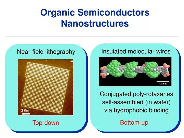
Insulated molecular wires. Near-field lithography. Conjugated poly-rotaxanes self-assembled (in water) via hydrophobic binding. Tool for embedding information into materials. Over a variety of Lengthscales. F Cacialli et al Nature Materials 1, 160 -164 (2002). R Riehn et al

E N D
Insulated molecular wires Near-field lithography Conjugated poly-rotaxanes self-assembled (in water) via hydrophobic binding Tool for embedding information into materials Over a variety of Lengthscales F Cacialli et al Nature Materials 1, 160 -164 (2002) R Riehn et al Applied Phys Lett82, 526-528 (2003) Organic Semiconductors Nanostructures Franco Cacialli Department of Physics and Astronomy, University College London (UCL) Gower Street, London, WC1E 6BT Patterning or the implementation of Shape is crucial to enable Function Bottom-up Top-down
Outline • Introduction • Patterning of organic semiconductors • Near-field direct lithography • Experiment • Results and simulations (Bethe-Bouwkamp) • Limitations • Insulated molecular wires • Supramolecular architectures • Optical and EL properties of conjugated rotaxanes • AFM morphology • Conclusions
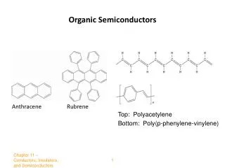
Conjugated Polymers Applications • Displays • Logic circuits • Photovoltaics • Sensors C.J. Drury, et al. Appl. Phys. Lett. 73, 108 (1998)
Motivation • Patterning* of organic semiconductors • RGB displays • Integrated low-cost electronics • Photonic structures • Nanodevices • Problems: • Minimise damage • Obtain the desired resolution *S. Holdcroft, Advanced Materials 13, 1753-1765 (2001).
Motivation • Patterning* of organic semiconductors • RGB displays • Integrated low-cost electronics • Photonic structures • Nanodevices • Problems: • Minimise damage • Obtain the desired resolution *S. Holdcroft, Advanced Materials 13, 1753-1765 (2001).
Photonic crystals • Structures with a periodic refractive index • Periodicity allowed and forbidden bands for photon propagation (analogy with electrons in “real” crystals) • Manipulation of the photon density of states higher luminescence efficiency • Manipulation of the photon propagation loss-less waveguides, sharp-bends, optochips • Need patterning on /2n lengthscale • 1D PC DBR Planar FP cavities JD Joannopoulos, et al. “Photonic crystals” (Princeton University Press, 1995)
Al (R=80±3%) (A=18±3%) Ag (R=85±3%) (A =6±1%) PL PPV: 160nm ITO: 96 nm DBR Glass Planar Fabry-Perot Cavities 4 nm PL intensity (a.u.) • Structure with Ag and no ITO • External Gain ~ 23 ratio of forward intensity in and out the cavity at resonance • Absorption in the Ag mirror ~ 40 %, Overlap factor ~ 63 % • Total enhancement in forward direction and at resonance ~ 60 • PL Efficiency: 23 vs 28 % Wavelength (nm) J. Grüner, F. Cacialli and R.H. Friend, J. Appl. Phys. 80, 207 (1996). G.R. Hayes, F. Cacialli and R.T. Phillips, Phys. Rev. B 56, 4798 (1997). S.E. Burns, et al. Optic. Mater. 9, 18 (1998).
PPV nanolithography Corner Cube Interferometer RIE (Reactive Ion Etching) defined holographic grating of PPV onto an ITO substrate. The lateral resolution is ~ 300 nm. Mirror Sample PL eff: ~ 30% of the unpatterned film G. Gigli, R. Rinaldi, C. Turco, P. Visconti, R. Cingolani and F. Cacialli APL 73, 3926 (1998).
Alternatives? Problems with conventional far-field lithography techniques • High resolution achieved with high energy (short wavelength) beams • Relatively aggressive species in some of the steps
Problems with conventional far-field lithography techniques • High resolution achieved with high energy (short wavelength) beams • Relatively aggressive species in some of the steps No sacrificial resist needed Alternatives • Soft lithographies (not ideal for prototyping) • long time to prepare the master • cost of master • Direct optical patterning of a photosensitive polymer • Direct High resolution?
Near-field Optical Lithography SNOM: Sub-wavelength resolution source/detector • Implementation • Tapered optical fiber/apertured metallic coating • Sharp metallic tip to enhance field (apertureless/scattering) • Resolution • 12-300 nm depending on the probe • Not directly linked to the wavelength • Potential for high resolution with minimum material damage • Applications • Subwavelength Optical manufacturing and characterisation
Poly(p-phenylene vinylene) UV • Precursor polymer (soluble) • Thermal conversion to fully conjugated polymer (insoluble) • Luminescence in the green • Optical gain lasing • Elimination reaction also at/under: • Room Temperature • Vacuum • UV irradiation 220 ºC
PPV - Lithography Spin precursor fromsolution in MeOH Develop inMeOH 20 s Thermal conversionat 220⁰C Illuminate withSNOM at 325 nm Glass or ITO
Experimental details SEM image of a Jasco Probe SEM image of a Jasco Probe Etched fibre: double taper 10-3-10-4 throughput Etched fibre: double taper 10-3-10-4 throughput Metallised optical fibre with aperture ~50 nm Home-built instrument Tuning Fork feedback system Tip-sample distance~ 2.5 nm Sample ~ 40 nm thick Fibrecoupler Shutter Optical Fibre HeCd 325nm Power: few mW Sample
Proof of principle Exp. time PPV - precursor
Interference BS Laser M Developed precursor Fully conjugated polymer M Sample Spectral period = 905.54 nm 40 nm thick precursor, 330 nm periodicity square lattice, 10x10 μm2 image. Intentional absence of the central pillar implements a defect (doping) of the periodic structure. Periodic structures SNOM Versatility R. Riehn et al. APL 82,526-528 (2003)
Resolution Exp. time • Constant height • “Stable positioning” • ↓width with ↓exposure time • ↓height with ↓ exposure time • Unstable positioning – “sliding” • Approx. constant feature width
Resolution partially soluble - gel completely insoluble fully soluble glass glass
Phase-contrast Decreasing exposure time Decreasing exposure time Decreasing exposure time • Higher phase contrast around the edges of the features • Indicative of a difference in the viscoelastic properties of the material: Hard-centre and softer rim • Area fraction of hard-centre with exposure time Corroborates assignment the rim to the gel-like phase F. Cacialli et al. Ultramicroscopy (2004)
Natural logarithm of the electric field intensity Simulations • 2a=50 nm, d=40 nm, s= 2.5 nm, λ=325 nm. • The surface of constant intensity just touching the substrate has a width of 72 nm (52 nm) in the x (y) direction, • the minimum-size experimental feature is 180 nm (160 nm after conversion). • The gel phase must account for 110-130 nm of the total width. R. Riehn et al. APL 82,526-528 (2003)
Mass transport of fresh precursor into lithographed features • Expose the developed (but not fully converted) features to fresh precursor solution Dust Lithographic features Height [nm] UV Horizontal width 303.31 nm Aspect ratio ~0.83 mm Heat Enhancing feature-height & aspect ratio R Riehn & F Cacialli J Optics A (in press).
SNOM lithography • Best resolution to date: 160 nm FWHM for 40nm-thick film • Promising for photonic structure prototypes in the visible • Improvements by: • Smaller apertures, tip-sample distance • Apertureless/scattering geometry, 2-photon abs • Processing of thinner films ……. • Molecular engineering • Lower mol weight precursors • Higher solubility of partially exposed areas
Electroluminescent insulated molecular wires: cyclodextrin-threaded conjugated polyrotaxanes F. Cacialli et al. Nature Materials 1, 160 -164 (2002).
Supramolecular architectures 1. Control of interchain interactions - Red-shift and quenching of the luminescence 2. Control of molecular conformation 3. Facilitated manipulation for single-molecule electronics 4. Encapsulation of the conjugated chromophores - Protection against degradation or contamination 5. Water-soluble materials biocompatible structures? aqueous inks for ink-jet printing?
Suzuki coupling in water • Carboxylate or sulfonate chains • N up to 20 - 30 • Threading ratio: 0.9 -1.6 (from 1H NMR) Materials
Materials • Van der Waals surface of N=2 -CD-PPP • Incomplete shielding of the conjugate core by the CD rings • CD rings act as spacers with an external diam. of about 1.5 nm () • Ionisation potential for -CD-PDV (PDV) is 5.36 (5.20) eV (not very different from PPV/PDV)
Blue-shift of absorption and emission on adding cyclodextrin groups ↓ of packing interactions or sterically-driven ↑ in twist angle Altered polarisability of molecular environment Optical Properties of Thin Films
PL Efficiencies (thin films) X 4.3 X 15 Org-soluble PF with b – CD = 75% PF without CD = 5 % Increase in PL efficiency on adding cyclodextrin groups (greatest for PDV) First generation materials Ratio of PL eff. higher for samples with catalyst residues Is the CD insulation preventing charge transport? PPP with b - CD = 12 % PPP without CD = 11 % PF with b - CD = 7 % PF without CD = 5 % PDV with b - CD = 17 % PDV without CD = 4 % X 1.1 X 1.4
Are these materials electroluminescent? Polymer Ca electrode with Al capping layer Electrical connection ITO electrode Glass substrate Light LUMO e Energy e Light Does the “insulation” of the cyclodextrins prevent charge transport? h h HOMO Ca Polymer ITO Electroluminescence Place them in an LED structure.
Electroluminescence …. efficiency and luminance are higher up to high current densities
-CD-PPP conc -CD-PPP diluted PPP 4 nm 3 nm 10 nm 0 nm 0 nm 0 nm AFM morphology All films spin-coated on muscovite mica a) from conc. solution (50 g/ml): not closely packed b) from diluted solution (1 g/ml): single chains chains up to >100 nm c) Polydumbbell assembles in domains 1.1 nm high
Excitons/unitary charge PL eff. Singlets/excitons EL efficiency h-e balance • PL efficiency • Use more efficient chromophores • Dilute chromophores even further • Solid-state solutions • Problem: phase separation tend to reduce effectiveness • Injection barriers to improve hole-electron balance to improve exciton formation efficiency • Anode/cathode engineering (Brown et al JAP 2003) • LECs approach (Pei et al. Science 1995)
Light-emitting Electrochemical Cells (LECs) LECs EL polymer + PEO + salt JC De Mello, et al. PRB, 57, 12951 (1998)
Ionic groups Add ion transport material - polyethylene oxide (PEO) • Present on both solubilising chains and stoppers • They influence turn-on though do not dominate LEDs behaviour • If lucky and careful can use ions in rotaxanes/ref materials 1) to promote supramolecular polar interaction with matrix 2) to increase ion conc. at cathodic interface layer to thin barrier an facilitate electron-injection (LEC-like)
Electroluminescence Efficiencies The effect of PEO-addition Large increase (x 30 -300) in EL efficiencies on adding PEO for all materials.
EL Efficiency vs. PEO content Maximum EL efficiency with b-CD always higher than without. • Blend morphology may reduce diffusion to quenching sites. • PEO makes ions more mobile assisting injection. • PL efficiency increases with PEO (x 3 -10). Higher with b-CD
PL Efficiency vs. PEO content PL efficiency increases with PEO (x 3 -10) • Less PEO is needed for the polyrotaxanes Good miscibility of conjugated polyelectrolytes in PEO
a c b-CD-PPP b-CD-PPP/PEO 500nm 500nm b d 100nm 100nm PPP-Polyrotaxanes- PEO (50/50) 5 nm 0 nm
Supramolecular engineering • Poly-electrolytic nature of the materials: Polar/ionic interactions promote miscibility with PEO • reduced phase-separation • enhanced PL efficiency 2. Supramolecular threading • reduced intermolecular interactions and cofacial alignment • enhanced PL and EL efficiency 3. Presence of PEO allows efficient ion-transport • Light-emitting electrochemical cells (LECs) • Increase of 100 in EL efficiency
Collaborators A Petrozza, LJ Parrott, O Fenwick, G Latini, A Ambrosio, A Downes Department of Physics and Astronomy, UCL and London Centre for Nanotechnology A Petrozza, J Wilson, C Daniel, C Silva, RH Friend Cavendish Laboratory, Department of Physics, University of Cambridge J Michels, PN Taylor, HL Anderson Department of Chemistry, University of Oxford N Severin, P Samorí #, J Rabe Department of Physics, Humboldt University Berlin # New address: Istituto per la Sintesi Organica e la Fotoreattività, CNR Bologna and ISIS-Strasbourg L Sardone, G Marletta Department of Chemistry, University of Catania
Thanks to Thanks for your attention! • EPSRC • Royal Society • EC (Marie Curie) • British Council (Windsor Treaty)
Conjugated rotaxanes • Threading conjugated polymers through cyclodextrins: 1) Blue-shifts the luminescence by around 0.1 - 0.2 eV 2) Increases the PL efficiency by up to a factor of 4 3) Increases the EL efficiency by up to a factor of 2 4) Allows single-molecule deposition via spin-coating • Improvements by: 1) Increase of the PL efficiency in the solid state organic soluble materials 75% 2) Supramolecular ionic interactions: enhanced miscibility in PEO reduced tendency to phase separation LECs – like devices with 300-fold efficiency increase
Electroluminescence b-CD-PDV EL PDV EL Intensity (a.u.) 1.6 2.0 2.4 2.8 3.2 Energy (eV) EL spectra also blue-shifted for the rotaxinated materials
Electroluminescence 3500 120 10 240 3000 PDV b-CD-PDV 100 8 200 2500 ) ) 80 2 2 160 6 2000 Luminance (cd/m 60 Luminance (cd/m J (mA / cm 120 J (mA / cm 1500 4 40 1000 80 2 20 2 2 500 ) ) 40 0 0 0 0 1 2 3 4 5 6 7 8 0 2 4 6 8 10 12 14 16 Applied Voltage (V) Applied Voltage (V) As expected, CDs bring about an increase of the turn-on voltage and a decrease of the current density
Ionic groups Add ion transport material - polyethylene oxide (PEO) • Present on both solubilising chains and stoppers • They influence turn-on though do not dominate LEDs behaviour
Light-emitting Electrochemical Cells (LECs) JC De Mello, et al. PRB, 57, 12951 (1998)