Download

1 / 10
140 likes | 534 Views
FET BIASING. FET BIASING. The general relation ships that can be applied to the DC analysis of all FET amplifiers are I G 0 Amp I D =I S For JFETS and Depletion type MOSFETs Shockley’s equation is applied to relate the input and output quantities

E N D
FET BIASING The general relation ships that can be applied to the DC analysis of all FET amplifiers are IG 0 Amp ID=IS For JFETS and Depletion type MOSFETs Shockley’s equation is applied to relate the input and output quantities For E-MOSFETs the following equation is applicable
FIXED BIAS CONFIGURATION: The fixed bias arrangement for the N-channel JFET is Coupling capacitors(C1 and C2) are “open circuits “ for the DC analysis and low impedances(essentially short circuits) for the AC analysis .The Resistor RG is present to ensure that Vi appears at the input to the FET amplifier for the AC analysis for DC analysis
then the circuit is Applying KVL in the input loop then
Since VGG is fixed DC supply the voltage VGS is fixed magnitude The resulting level of Drain current ID is The Drain to source voltage can be determined by applying KVL to output loop
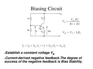
SELF BIASING: The self biasing configuration eliminates the need for two DC supplies The controlling gate-to-source voltage is now determined by the voltage across RS For DC analysis the capacitors can again be replaced by “open circuits “ and RG is replaced by a short circuit equivalent since IG=0 then the circuit becomes Current passing through RS is VRS=IDRS Apply KVL in input loop then -VGS-VRS=0 VGS=-IDRS Then
Apply KVL to the output loop then Q-point (VGS, ID) VDD-IDRD-VDS-IDRS=0 VDS=VDD-ID(RD+RS) VS=IDRS VG=0 then VD=VDS+VS (or) VDD-VR
VOLTAGE –DIVIDER BIASING: For DC analysis , all capacitors replaced by open circuits and IG=0,So that current passing through R1 and R2 same (IR) then VG=VDD ---------> 1 Apply KVL to the input loop then VG-VGS-IDRS=0 VGS=VG-IDRS----------> 2 Substitute in ID then - --------> 3
Apply KVL to output loop then VDD-IDRD-VDS-IDRS=0 VDS=VDD-ID(RD+RS)---------> 4 Then VD=VDS+VS (or) VD =VDD-IDRD Vs=IDRS