Download
1 / 39
510 likes | 1.05k Views
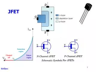
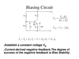
JFET Biasing. ENGI 242/ELEC 222. JFET Fixed Bias. R G is present to limit current in case V GG is connected with wrong polarity This would forward bias the gate-source junction causing high currents, which would destroy the transistor. Since GS is reverse biased, I G = 0 and V RG = 0.

E N D
JFET Biasing ENGI 242/ELEC 222
JFET Fixed Bias RG is present to limit current in case VGG is connected with wrong polarity This would forward bias the gate-source junction causing high currents, which would destroy the transistor Since GS is reverse biased, IG = 0 and VRG = 0 ENGI 242/ELEC 222
DC Analysis for JFET Fixed Bias Network ENGI 242/ELEC 222
JFET Fixed Bias Plotting Shockley’s Equation ENGI 242/ELEC 222
JFET Fixed Bias Graphical Solution ENGI 242/ELEC 222
JFET Fixed Bias ENGI 242/ELEC 222
Graphical Solution for JFET Fixed Bias ENGI 242/ELEC 222
JFET Self Bias Configuration ENGI 242/ELEC 222
JFET Self Bias DC Equivalent Circuit IG = 0 VRG = 0 ENGI 242/ELEC 222
Transconductance Curve ENGI 242/ELEC 222
JFET Self Bias Load Line ENGI 242/ELEC 222
JFET Self Bias ENGI 242/ELEC 222
JFET Self Bias Transconductance Curve ENGI 242/ELEC 222
Graphical Solution of JFET Self Bias ENGI 242/ELEC 222
JFET Self Bias Effect on Variation of RS ENGI 242/ELEC 222
Self Bias ENGI 242/ELEC 222
JFET Voltage Divider Bias ENGI 242/ELEC 222
JFET Voltage Divider Bias DC Analysis Input Output ENGI 242/ELEC 222
JFET Voltage Divider Bias Load Line ENGI 242/ELEC 222
The Effect of RS on Q-point ENGI 242/ELEC 222
JFET Voltage Divider Bias ENGI 242/ELEC 222
JFET Voltage Divider Bias Q-point ENGI 242/ELEC 222
Voltage Divider Bias ENGI 242/ELEC 222
MOSFET Biasing ENGI 242/ELEC 222
D-MOSFET Self Bias ENGI 242/ELEC 222
Determining the Q-point for D-MOSFET Self Bias ENGI 242/ELEC 222
NChannel D-MOSFET Voltage Divider Bias ENGI 242/ELEC 222
Q Point of D-MOSFET Voltage Divider Bias ENGI 242/ELEC 222
Effect on Change in Q Point with Variation of RS With an N Channel D-MOSFET, VGS may be positive ENGI 242/ELEC 222
D-MOSFET Fixed Bias ENGI 242/ELEC 222
E-MOSFET Feedback Bias ENGI 242/ELEC 222
DC Equivalent For the E-MOSFET Feedback Bias IG = 0 VGS = VDS ENGI 242/ELEC 222
Transfer Curve for the E-MOSFET Feedback Bias ENGI 242/ELEC 222
Determining the Q-point for E-MOSFET Feedback Bias ENGI 242/ELEC 222
Q-point for the E-MOSFET Fixed Bias ENGI 242/ELEC 222
EMOS Feedback Bias Example VGSTH = 4V VGSon = 7.5V IDon = 5mA VDD = 22V ENGI 242/ELEC 222
EMOS Feedback Example ENGI 242/ELEC 222
Voltage Divider Bias for an N E-MOSFET ENGI 242/ELEC 222
Q-point for E-MOSFET Voltage Divider Bias ENGI 242/ELEC 222