Download
1 / 9
90 likes | 183 Views
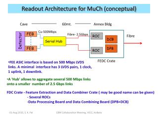
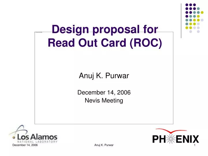
Design proposal for Read Out Card (ROC). Anuj K. Purwar December 14, 2006 Nevis Meeting. Functionality. Read in serial data from N FPIX chips via 1, 2 or 4 LVDS pairs, strip off sync words, process and combine data words from several FPIX into a single 28-bit parallel stream to SERDES.

E N D
Design proposal for Read Out Card (ROC) Anuj K. Purwar December 14, 2006 Nevis Meeting Anuj K. Purwar
Functionality • Read in serial data from N FPIX chips via 1, 2 or 4 LVDS pairs, strip off sync words, process and combine data words from several FPIX into a single 28-bit parallel stream to SERDES. • Send FPIX control signals e.g. FFR and supply BCO clock and Readout clock to FPIX. • Send pulses for calibration. • Implement slow control interface with FEM to download commands. • Radiation tolerant (if sitting in IR). Anuj K. Purwar
Calibration System Calibration pulse ROC command FPIX control ROC State Machine Download data 28-bit word FPIX 1 Deserializer Channel Combiner FIFO FPIX N BCO Clock Digital Clock Manager BCO Clock Readout Clock ROC Block Diagram Anuj K. Purwar
Implementation details • Deserializer: Uses shift registers to convert LVDS serial stream into 24-bit parallel words and appends a 4-bit Chip ID. • Channel Combiner: Uses a multiplexer and counter to combine the 28-bit words from N deserializers into a single stream. It then strips off the sync words and sends the data words into the FIFO. • FIFO: Buffers data words and sends them to SERDES. • Calibration: Talks to Pat’s calibration board and sets pulse height/timing. • Command FSM (Finite State Machine): Receives commands via USB (slow control) and sends appropriate responses to FPIX and internal components (like send data). Anuj K. Purwar
Segmentation • FPIX to fiber mapping depends primarily upon latency/throughput requirements. • Details worked out by Sergey: Anuj K. Purwar
8-chip HDI USB Interface Actel Starter Board Lab setup Anuj K. Purwar
1 line each from 4 chips Chip ID from sync word SendData enabled for Chip ID = 4 Chip ID appended by FPGA Data is Valid Current “8 chip” module • Using Actel Starter kit with A3P250 chip. • Can successfully readout 4 chips and combine into a single data stream (24+3 bit wide). • Slow controls via USB. Anuj K. Purwar
Multiple line readout of 1 chip • Can read out 4 lines successfully. • Slow controls implemented via USB. 4 lines New words Alines = 10 RejectHits SendData Anuj K. Purwar
To do • Ordered a sample Actel A3PE600 chip to replace existing A3P250 chip on the Actel Starter board. • 20 available LVDS pairs allowing up to 2 line readout of 8-chip module. • Need a fully working 8 chip module. • Just got National Instruments DigitalIO PCI card (NI 6534) which can do 32-bit data acquisition at 20 MHz which corresponds to 640 Mbps). Anuj K. Purwar