Download
1 / 6
70 likes | 307 Views
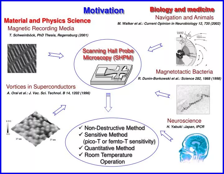
Motivation. Biology and medicine. Navigation and Animals. Material and Physics Science. M. Walker et al.: Current Opinion in Neurobiology 12, 735 (2002). Magnetic Recording Media. T. Schweinb öck, PhD Thesis, Regensburg (2001). Scanning Hall Probe Microscopy (SHPM).

E N D
Motivation Biology and medicine Navigation and Animals Material and Physics Science M. Walker et al.: Current Opinion in Neurobiology 12, 735 (2002) Magnetic Recording Media T. Schweinböck, PhD Thesis, Regensburg (2001) Scanning Hall Probe Microscopy (SHPM) Magnetotactic Bacteria R. Dunin-Borkowski et al.: Science 282, 1868 (1998) Vortices in Superconductors A. Oral et al.: J. Vac. Sci. Technol. B 14, 1202 (1996) Neuroscience H. Yabuki :Japan, IPCR • Non-Destructive Method • Sensitive Method (pico-T or femto-T sensitivity) • Quantitative Method • Room Temperature Operation
d = 0 nm (sample A) d = 1.0 nm (sample B) d = 1.5 nm (sample C) d = 2.0 nm (sample D) ND1 = 8 1017 cm-3 ND2 = 3 1018 cm-3 5 nm In0.53Ga0.47As:Si, ND2 25 nm In0.52Al0.48As 15 nm In0.53Ga0.47As:Si, ND1 d nm InAs 15 nm In0.53Ga0.47As:Si, ND1 20 nm In0.52Al0.48As InP:Fe (100) substrate Material Growth by MBE and Device Design Au/Ge/Ni contact pads Greek Cross Device Active Area
Contact Optimization by Transmission Line Model lT c c Au/Ge/Ni d rs Rs Rs dx Dopant 0 -l x Processed TLM Structure Au/Ge/Ni contact pads
Hall Effect Measurements: Non-linearity studies • Development of temperature stable magnetosensor by channel doping • High signal linearity at low and high electric fields
Absolute Magnetic Sensitivity and Noise Studies • Insertion of InAs into InGaAs QW increases the magnetic sensitivity • Further noise studies required for G-R source identification to lower background noise
Conclusions & Future Work • Quantum well micro-Hall sensors based on high-electron drift velocity materials are successfully fabricated • Insertion of strained InAs QW into the lattice matched In0.52Al0.48As/In0.53Ga0.47As heterostructure results in sensitivity increase • Further noise studies are required to clarify origins of generation- recombination noise • Optimization of heterostructure is required for obtaining low thermal drift, higher magnetic sensitivity and lower background noise • Magnetic field resolution in nanotesla range by 10 m micro-Hall sensors is expected