Download
1 / 32
320 likes | 344 Views
This guide explains the role of datapath and control unit in processor design, covering R-type, lw, sw, and beq instructions with relevant signal paths and control signal generation. Learn about the single-cycle datapath implementation in MIPS architecture.

E N D
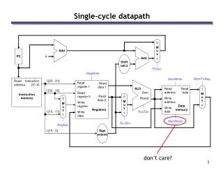
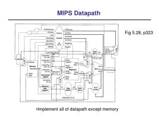
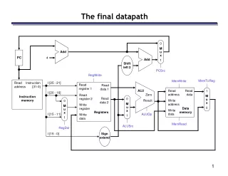
0 M u x 1 Add PC 4 Add Shift left 2 PCSrc RegWrite MemToReg MemWrite Read address Instruction [31-0] I [25 - 21] Read register 1 Read data 1 ALU Read address Read data 1 M u x 0 I [20 - 16] Zero Read register 2 Instruction memory Read data 2 0 M u x 1 Result Write address 0 M u x 1 Write register Data memory Write data Registers I [15 - 11] ALUOp Write data MemRead ALUSrc RegDst I [15 - 0] Sign extend The final datapath
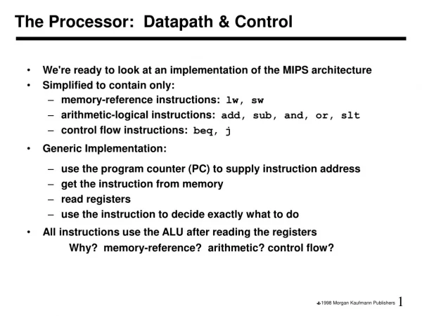
Control • The control unit is responsible for setting all the control signals so that each instruction is executed properly. • The control unit’s input is the 32-bit instruction word. • The outputs are values for the blue control signals in the datapath. • Most of the signals can be generated from the instruction opcode alone, and not the entire 32-bit word. • To illustrate the relevant control signals, we will show the route that is taken through the datapath by R-type, lw, sw and beq instructions.
0 M u x 1 Add PC 4 Add Shift left 2 PCSrc RegWrite MemToReg MemWrite Read address Instruction [31-0] I [25 - 21] Read register 1 Read data 1 ALU Read address Read data 1 M u x 0 I [20 - 16] Zero Read register 2 Instruction memory Read data 2 0 M u x 1 Result Write address 0 M u x 1 Write register Data memory Write data Registers I [15 - 11] ALUOp Write data MemRead ALUSrc RegDst I [15 - 0] Sign extend R-type instruction path • The R-type instructions include add, sub, and, or, and slt. • The ALUOp is determined by the instruction’s “func” field.
0 M u x 1 Add PC 4 Add Shift left 2 PCSrc RegWrite MemToReg MemWrite Read address Instruction [31-0] I [25 - 21] Read register 1 Read data 1 ALU Read address Read data 1 M u x 0 I [20 - 16] Zero Read register 2 Instruction memory Read data 2 0 M u x 1 Result Write address 0 M u x 1 Write register Data memory Write data Registers I [15 - 11] ALUOp Write data MemRead ALUSrc RegDst I [15 - 0] Sign extend lw instruction path • An example load instruction is lw $t0, –4($sp). • The ALUOp must be 010 (add), to compute the effective address.
0 M u x 1 Add PC 4 Add Shift left 2 PCSrc RegWrite MemToReg MemWrite Read address Instruction [31-0] I [25 - 21] Read register 1 Read data 1 ALU Read address Read data 1 M u x 0 I [20 - 16] Zero Read register 2 Instruction memory Read data 2 0 M u x 1 Result Write address 0 M u x 1 Write register Data memory Write data Registers I [15 - 11] ALUOp Write data MemRead ALUSrc RegDst I [15 - 0] Sign extend sw instruction path • An example store instruction is sw $a0, 16($sp). • The ALUOp must be 010 (add), again to compute the effective address.
0 M u x 1 Add PC 4 Add Shift left 2 PCSrc RegWrite MemToReg MemWrite Read address Instruction [31-0] I [25 - 21] Read register 1 Read data 1 ALU Read address Read data 1 M u x 0 I [20 - 16] Zero Read register 2 Instruction memory Read data 2 0 M u x 1 Result Write address 0 M u x 1 Write register Data memory Write data Registers I [15 - 11] ALUOp Write data MemRead ALUSrc RegDst I [15 - 0] Sign extend beq instruction path • One sample branch instruction is beq $at, $0, offset. • The ALUOp is 110 (subtract), to test for equality. The branch may or may not be taken, depending on the ALU’s Zero output
Control signal table • sw and beq are the only instructions that do not write any registers. • lw and sw are the only instructions that use the constant field. They also depend on the ALU to compute the effective memory address. • ALUOp for R-type instructions depends on the instructions’ func field. • The PCSrc control signal (not listed) should be set if the instruction is beq and the ALU’s Zero output is true.
RegWrite ALUOp MemWrite RegDst I [31 - 26] ALUSrc I [5 - 0] MemToReg Read address Instruction [31-0] Control Instruction memory MemRead PCSrc Zero Generating control signals • The control unit needs 13 bits of inputs. • Six bits make up the instruction’s opcode. • Six bits come from the instruction’s func field. • It also needs the Zero output of the ALU. • The control unit generates 10 bits of output, corresponding to the signals mentioned on the previous page. • You can build the actual circuit by using big K-maps, big Boolean algebra, or big circuit design programs. • The textbook presents a slightly different control unit.
Summary - Single Cycle Datapath • A datapath contains all the functional units and connections necessary to implement an instruction set architecture. • For our single-cycle implementation, we use two separate memories, an ALU, some extra adders, and lots of multiplexers. • MIPS is a 32-bit machine, so most of the buses are 32-bits wide. • The control unit tells the datapath what to do, based on the instruction that’s currently being executed. • Our processor has ten control signals that regulate the datapath. • The control signals can be generated by a combinational circuit with the instruction’s 32-bit binary encoding as input. • Now we’ll see the performance limitations of this single-cycle machine and try to improve upon it.
Multicycle datapath • We just saw a single-cycle datapath and control unit for our simple MIPS-based instruction set. • A multicycle processor fixes some shortcomings in the single-cycle CPU. • Faster instructions are not held back by slower ones. • The clock cycle time can be decreased. • We don’t have to duplicate any hardware units. • A multicycle processor requires a somewhat simpler datapath which we’ll see today, but a more complex control unit that we’ll see later.
The example add from last time • Consider the instruction add $s4, $t1, $t2. • Assume $t1 and $t2 initially contain 1 and 2 respectively. • Executing this instruction involves several steps. • The instruction word is read from the instruction memory, and the program counter is incremented by 4. • The sources $t1 and $t2 are read from the register file. • The values 1 and 2 are added by the ALU. • The result (3) is stored back into $s4 in the register file.
1 M u x 0 0 M u x 1 Add Add Shift left 2 PCSrc MemToReg MemWrite Read address Instruction [31-0] Read register 1 Read data 1 PC ALU Read address Read data Zero Read register 2 Instruction memory Read data 2 Write address Result 0 M u x 1 0 M u x 1 Write register Data memory Write data Registers ALUOp Write data MemRead ALUSrc RegDst Sign extend I [15 - 0] How the add goes through the datapath PC+4 4 RegWrite I [25 - 21] 01001 00...01 I [20 - 16] 01010 00...10 I [15 - 11] 10100 00...11
MemWrite Read register 1 Read data 1 PC Read address Read data Read register 2 RegWrite Read data 2 Write address Write register Data memory Write data Registers Write data MemRead State elements • In an instruction like add $t1, $t1, $t2, how do we know $t1 is not updated until after its original value is read?
The datapath and the clock • STEP 1: A new instruction is loaded from memory. The control unit sets the datapath signals appropriately so that • registers are read, • ALU output is generated, • data memory is read and • branch target addresses are computed. • STEP 2: • The register file is updated for arithmetic or lw instructions. • Data memory is written for a sw instruction. • The PC is updated to point to the next instruction. • In a single-cycle datapath everything in Step 1 must complete within one clock cycle.
1 M u x 0 reading the instruction memory 2ns reading the base register $sp 1ns computing memory address $sp-4 2ns reading the data memory 2ns storing data back to $t0 1ns I [25 - 21] 8ns Read address Instruction [31-0] Read register 1 Read data 1 ALU Read address Read data I [20 - 16] Zero Read register 2 Instruction memory Read data 2 Result Write address 0 M u x 1 0 M u x 1 Write register Data memory Write data Registers I [15 - 11] Write data Sign extend I [15 - 0] The slowest instruction... • If all instructions must complete within one clock cycle, then the cycle time has to be large enough to accommodate the slowest instruction. • For example, lw $t0, –4($sp) needs 8ns, assuming the delays shown here. 2 ns 2 ns 0 ns 2 ns 0 ns 0 ns 1 ns 0 ns
1 M u x 0 reading the instruction memory 2ns reading registers $t1 and $t2 1ns computing $t1 + $t2 2ns storing the result into $s0 1ns 6ns I [25 - 21] Read address Instruction [31-0] Read register 1 Read data 1 ALU Read address Read data I [20 - 16] Zero Read register 2 Instruction memory Read data 2 Result Write address 0 M u x 1 0 M u x 1 Write register Data memory Write data Registers I [15 - 11] Write data 2 ns Sign extend 2 ns 0 ns 2 ns I [15 - 0] 0 ns 0 ns 1 ns 0 ns ...determines the clock cycle time • If we make the cycle time 8ns then every instruction will take 8ns, evenif they don’t need that much time. • For example, the instruction add $s4, $t1, $t2 really needs just 6ns.
How bad is this? • With these same component delays, a sw instruction would need 7ns, and beq would need just 5ns. • Let’s consider the gcc instruction mix from p. 189 of the textbook. • With a single-cycle datapath, each instruction would require 8ns. • But if we could execute instructions as fast as possible, the average time per instruction for gcc would be: (48% x 6ns) + (22% x 8ns) + (11% x 7ns) + (19% x 5ns) = 6.36ns • The single-cycle datapath is about 1.26 times slower!
It gets worse... • We’ve made very optimistic assumptions about memory latency: • Main memory accesses on modern machines is >50ns. • For comparison, an ALU on the Pentium4 takes ~0.3ns. • Our worst case cycle (loads/stores) includes 2 memory accesses • A modern single cycle implementation would be stuck at <10Mhz. • Caches will improve common case access time, not worst case. • Tying frequency to worst case path violates first law of performance!!
A multistage approach to instruction execution • We’ve informally described instructions as executing in several steps. • Instruction fetch and PC increment. • Reading sources from the register file. • Performing an ALU computation. • Reading or writing (data) memory. • Storing data back to the register file. • What if we made these stages explicit in the hardware design?
Performance benefits • Each instruction can execute only the stages that are necessary. • Arithmetic • Load • Store • Branches • This would mean that instructions complete as soon as possible, instead of being limited by the slowest instruction. • Proposed execution stages • Instruction fetch and PC increment • Reading sources from the register file • Performing an ALU computation • Reading or writing (data) memory • Storing data back to the register file
The clock cycle • Things are simpler if we assume that each “stage” takes one clock cycle. • This means instructions will require multiple clock cycles to execute. • But since a single stage is fairly simple, the cycle time can be low. • For the proposed execution stages below and the sample datapath delays shown earlier, each stage needs 2ns at most. • This accounts for the slowest devices, the ALU and data memory. • A 2ns clock cycle time corresponds to a 500MHz clock rate! • Proposed execution stages • Instruction fetch and PC increment • Reading sources from the register file • Performing an ALU computation • Reading or writing (data) memory • Storing data back to the register file
Cost benefits • As an added bonus, we can eliminate some of the extra hardware from the single-cycle datapath. • We will restrict ourselves to using each functional unit once per cycle, just like before. • But since instructions require multiple cycles, we could reuse some units in a different cycle during the execution of a single instruction. • For example, we could use the same ALU: • to increment the PC (first clock cycle), and • for arithmetic operations (third clock cycle). • Proposed execution stages • Instruction fetch and PC increment • Reading sources from the register file • Performing an ALU computation • Reading or writing (data) memory • Storing data back to the register file
Two extra adders • Our original single-cycle datapath had an ALU and two adders. • The arithmetic-logic unit had two responsibilities. • Doing an operation on two registers for arithmetic instructions. • Adding a register to a sign-extended constant, to compute effective addresses for lw and sw instructions. • One of the extra adders incremented the PC by computing PC + 4. • The other adder computed branch targets, by adding a sign-extended, shifted offset to (PC + 4).
0 M u x 1 1 M u x 0 Shift left 2 PCSrc RegWrite MemToReg MemWrite I [25 - 21] Read address Instruction [31-0] Read register 1 Read data 1 PC Read address Read data I [20 - 16] Read register 2 Instruction memory Read data 2 Write address 0 M u x 1 0 M u x 1 Write register Data memory Write data Registers I [15 - 11] Write data MemRead ALUSrc RegDst Sign extend I [15 - 0] The extra single-cycle adders Add 4 Add ALU Zero Result ALUOp
Our new adder setup • We can eliminate both extra adders in a multicycle datapath, and instead use just one ALU, with multiplexers to select the proper inputs. • A 2-to-1 mux ALUSrcA sets the first ALU input to be the PC or a register. • A 4-to-1 mux ALUSrcB selects the second ALU input from among: • the register file (for arithmetic operations), • a constant 4 (to increment the PC), • a sign-extended constant (for effective addresses), and • a sign-extended and shifted constant (for branch targets). • This permits a single ALU to perform all of the necessary functions. • Arithmetic operations on two register operands. • Incrementing the PC. • Computing effective addresses for lw and sw. • Adding a sign-extended, shifted offset to (PC + 4) for branches.
PC IorD RegDst RegWrite Read register 1 Read data 1 Read register 2 Address Read data 2 0 M u x 1 0 M u x 1 0 M u x 1 Write register Memory Write data Registers Write data Mem Data MemToReg The multicycle adder setup highlighted PCWrite ALUSrcA MemRead 0 M u x 1 ALU Zero Result 0 1 2 3 4 ALUOp MemWrite ALUSrcB Sign extend Shift left 2
Eliminating a memory • Similarly, we can get by with one unified memory, which will store both program instructions and data. (a Princeton architecture) • This memory is used in both the instruction fetch and data access stages, and the address could come from either: • the PC register (when we’re fetching an instruction), or • the ALU output (for the effective address of a lw or sw). • We add another 2-to-1 mux, IorD, to decide whether the memory is being accessed for instructions or for data. • Proposed execution stages • Instruction fetch and PC increment • Reading sources from the register file • Performing an ALU computation • Reading or writing (data) memory • Storing data back to the register file
PCWrite Shift left 2 IorD MemRead ALUSrcA PC 0 M u x 1 RegDst RegWrite Read register 1 Read data 1 ALU Read register 2 Zero Address Read data 2 4 0 1 2 3 Result 0 M u x 1 0 M u x 1 0 M u x 1 Write register MemWrite Memory ALUOp Write data Registers Write data Mem Data ALUSrcB Sign extend MemToReg The new memory setup highlighted
Intermediate registers • Sometimes we need the output of a functional unit in a later clock cycle during the execution of one instruction. • The instruction word fetched in stage 1 determines the destination of the register write in stage 5. • The ALU result for an address computation in stage 3 is needed as the memory address for lw or sw in stage 4. • These outputs will have to be stored in intermediate registers for future use. Otherwise they would probably be lost by the next clock cycle. • The instruction read in stage 1 is saved in Instruction register. • Register file outputs from stage 2 are saved in registers A and B. • The ALU output will be stored in a register ALUOut. • Any data fetched from memory in stage 4 is kept in the Memory data register, also called MDR.
PCSource Shift left 2 ALUSrcA PC IorD RegDst IRWrite RegWrite A Read register 1 Read data 1 ALU B Read register 2 Zero Address Read data 2 [31-26] [25-21] [20-16] [15-11] [15-0] 0 1 2 3 Result 0 M u x 1 0 M u x 1 0 M u x 1 0 M u x 1 0 M u x 1 Write register Memory ALUOp Write data Registers Write data Mem Data Instruction register ALUSrcB Memory data register Sign extend MemToReg The final multicycle datapath PCWrite MemRead ALU Out 4 MemWrite
Register write control signals • We have to add a few more control signals to the datapath. • Since instructions now take a variable number of cycles to execute, we cannot update the PC on each cycle. • Instead, a PCWrite signal controls the loading of the PC. • The instruction register also has a write signal, IRWrite. We need to keep the instruction word for the duration of its execution, and must explicitly re-load the instruction register when needed. • The other intermediate registers, MDR, A, B and ALUOut, will store data for only one clock cycle at most, and do not need write control signals.
Summary • A single-cycle CPU has two main disadvantages. • The cycle time is limited by the worst case latency. • It requires more hardware than necessary. • A multicycle processor splits instruction execution into several stages. • Instructions only execute as many stages as required. • Each stage is relatively simple, so the clock cycle time is reduced. • Functional units can be reused on different cycles. • We made several modifications to the single-cycle datapath. • The two extra adders and one memory were removed. • Multiplexers were inserted so the ALU and memory can be used for different purposes in different execution stages. • New registers are needed to store intermediate results. • Next time, we’ll look at controlling this datapath.