Download
1 / 17
170 likes | 273 Views
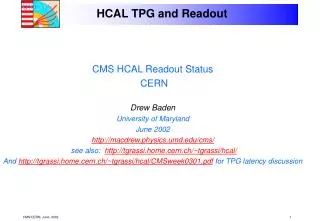
HCAL TPG and Readout. CMS HCal meeting at Rochester Oct. 19-20 Oct 2001 Tullio Grassi, Drew Baden University of Maryland Jim Rohlf Boston University. Level 1 Trigger. Detector Front End. Readout Crates. Online Controls. Event Manager. Event Builder. Level 2/3 Filter Units.

E N D
HCAL TPG and Readout CMS HCal meeting at Rochester Oct. 19-20 Oct 2001 Tullio Grassi, Drew Baden University of Maryland Jim Rohlf Boston University HCAL TriDAS
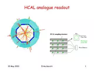
Level 1 Trigger Detector Front End Readout Crates Online Controls Event Manager Event Builder Level 2/3 Filter Units Computing Services CMS TriDAS Architecture • Data from CMS FE to T/DAQ Readout Crates • Level 1 “primitives” • Crossing determined • Summing • Tx to Level 1 Trigger • Data is pipelined waiting decision • Level 1 accepts cause • Tx raw data to concentrators • Buffered and wait for DAQ readout • System communication via separate path (TTC) • Clock, resets, errors, L1 accepts… HCAL TriDAS
HCAL Contribution to T/DAQ • Includes: • Receiver cards ( including fiber input receivers and deserializers) • Cables to Level 1 Trigger system • Concentrators • VME crate CPU module • VME crates and racks • Everything between but not including: • Fibers from QIE FEs • DAQ cables Trigger/DAQ Front End Readout Crate - Level 1 Buffer - Level 2 Concentrator - Crate CPU Level 2 and DAQ CMS HCAL HCAL Data QIE Fibers Level 1 Trigger HCAL TriDAS
Trigger Primitives READ-OUT Crate (in UXA) DAQ DATA SLINK64 [1 Gbit/s] CAL REGIONAL TRIGGER CPU D C C H T R H T R H T R DAQ RUI 18 HTRs per Readout Crate 16 bits @ 80 MHz TTC 32 bits @ 40 MHz CCA CCA CCA FRONT-END RBX Readout Box (On detector) HPD Shield Wall QIE GOL QIE QIE Fibers at 1.6 Gb/s 3 QIE-channels per fiber QIE GOL QIE QIE FE MODULE HCAL FE/DAQ Overview HCAL TriDAS
Front End Electronics TTC fiber Gbit Ethernet @ 1.6 Gb/s F a n O u t B I T 3 H TR H T R H T R H T R D C C ... 20 m Copper Links 1 Gb/s DAQ Calorimeter Regional Trigger Readout Crate Components • “BIT3” board • Commercial VME/PCI Interface to CPU • Slow monitoring • FanOut board • FanOut of TTC stream • FanOut of RX_CK & RX_BC0 • HTR (HCAL Trigger and Readout) board • FE-Fiber input • TPs output (SLBs) to CRT • DAQ/TP Data output to DCC • Spy output • DCC (Data Concentrator Card) board • Input from HTRs • Output to DAQ • Spy output D C C HCAL TriDAS
HCALTRIGGERandREADOUTCard • I/O on front panel: • Inputs: Raw data: • 16 digital serial fibers from QIE, 3 HCAL channels per fiber = 48 HCAL channels • Inputs: Timing (clock, orbit marker, etc.) • LVDS • Outputs: DAQ data output to DCC • Two connector running LVDS • TPG (Trigger Primitive Generator, HCAL Tower info to L1) via P2/P3 • Via shielded twisted pair/Vitesse • Use aux card to hold Tx daughterboards • FPGA logic implements: • Level 1 Path: • Trigger primitive preparation • Transmission to Level 1 • Level 2/DAQ Path: • Buffering for Level 1 Decision • No filtering or crossing determination necessary • Transmission to DCC for Level 2/DAQ readout HCAL TriDAS
HTR – “Dense” scheme Throughput: 17 Gb/s Latency: + 2 TCK DeS DeS DeS P1 FPGA Xilinx Vertex-2 SLB -PMC OPTICAL Rx (8 LC) DeS 8 FE fibers 24 QIE-ch’s DeS SLB -PMC DeS P2 LVDS Tx DeS DeS to DCC SLB -PMC Trigger output 48 Trigger Towers DeS DeS SLB -PMC DeS FPGA Xilinx Vertex-2 DeS OPTICAL Rx (8 LC) SLB -PMC 8 FE fibers 24 QIE-ch’s DeS P3 DeS SLB -PMC to DCC LVDS Tx DeS DeS 9U Board HCAL TriDAS
“Dense” HTR • Strong reasons to push to dense scheme • Money • Fewer boards! • Programmable logic vs. hardware • Avoid hardware MUXs • Maintain synchronicity • Single FPGA per 8 channels • Both L1/TPG and L1A/DCC processing • Xilinx Vertex-2 PRO will have deserializer chips built in! • Saves $500/board • Many fewer connections • ~20 DeS->FPGA connections replaced by 1 1.6 GHz line • Challenges: • Layout of 1.6 GHz signals • Schedule implications for final production may have to slip ~6 months to wait for Vertex-2 PRO • What do we give up? • Each board much more epensive • More difficult layout • Need transition board to handle TPG output • So does ECAL – common solution will be used • Need 2 DCC/crate (but half the number of crates!) HCAL TriDAS
Changes from HTR Demo to Final • Front-end input • From 800MHz HP G-Links to 1600MHz TI Gigabit ethernet • Timing • TTC daughterboard to TTC ASIC • Core logic • Altera to Xilinx • Trigger output • Moved to transition board • Form factor • 6U to 9U Output to DCC? Unchanged!!! HCAL TriDAS
Status • Front-end emulator HTR demonstrator DCC S-Link CPU • Successful operation of each individual link • Integration underway - Tullio goes to Boston next week • Pre-prototype board layout • Complete, board is now being stuffed • Will have only 1 FPGA with full complement of associated parts • Will use the TI Deserializers – not the Vertex 2 PRO • Internal use only • Prototype layout • Should be complete in November • Some changes from pre-prototype, but minor • Maryland activity is in prep for source tests and 9U board design • Preparation for testbeam summer 02 not yet started • Trying hard to meet March 02 deadline for decision on which HTR to use for testbeam • Energy filters still undefined HCAL TriDAS
Current HTR Timeline HCAL TriDAS
PCI Interfaces PMC Logic Board Buffers 1000 Events P2 P0 P1 6 PC-MIP mezzanine cards - 3 LVDS Rx per card Data from 18 HTR cards CERN S-Link Interface with DAQ To DAQ DATACONCENTRATORCARD Motherboard/daughterboard design: • Build motherboard to accommodate • PCI interfaces (to PMC and PC-MIP) • VME interface • PC-MIP cards for data input • 3 LVDS inputs per card • 6 cards per DCC (= 18 inputs) • Engineering R&D courtesy of D • 1 PMC cards for • Buffering: • Transmission to L2/DAQ via CERN S-Link Tx • http://hsi.web.cern.ch/HSI/s-link/ HCAL TriDAS
Project Status Details DCC@BU DCC Logic Board TTCRx Xilinx VirtexII XC2V1000 2Mx32 DDRSDRAM S-Link Source Card (optical fibre to DAQ) • VME Motherboard • Two prototypes working; 5 more boards being built • Link Receiver Board (LRB) • 10 second-generation boards working • DCC Logic Board • PCB Design complete; being fabricated • FPGA coding underway • Test Stand Hardware Complete • Pentium/Linux computer, TTC System Working • Link Transmitters to simulate HRC working • S-Link cards available 3-Channel LVDS Serial Link Receiver (6 used in final DCC) PC-MIP PCI standard Companion LVDS Serial Link Transmitter (for testing only) HCAL TriDAS
HCALTIMINGFANOUTModule • Fanout of TTC info: • Both TTC channels fanout to each HTR and DCC • Separate fanout of clock/BC0 for TPG synchronization • “daSilva” scheme • Single width VME module HCAL TriDAS
Cern Test Beam FNAL source calib. Slice Test I Slice Test II Current Project Timeline 2000 2001 2002 2003 2004 Demonstrator Requirements Resources Links 6U board Prototype New I/Os Simple Algorithms Pre-Prod Corner cases, HF heavy ions Production Test bench Pre-prod too short: not useful Test bench before production ? Slice Test I with pre-production ? Vertex-2 PRO? STILL SOME UNCERTAINTIES… HCAL TriDAS
Weiming Qian Engineer Univ. of Ill, Chicago Full-time Drew Baden Physicist University of Maryland Level 3 Manager Mark Adams Drew Baden Jim Rohlf Physicist Physicist Physicist Univ. of Ill, Chicago University of Maryland Boston University Suichi Kunori Chris Tully Sarah Eno DCC Task HTR Task HRC Task Physicist Physicist Physicist UMD UMD Princeton University Eric Hazen Rob Bard Jack Touart Hans Breden Rich Baum John Giganti Salavat Abdoulinne Silvia Arcelli Senior Engineer Engineer Engineer Senior Engineer Engineer Senior Engineer Post-Doc Post-Doc UMD BU UMD UMD UMD UMD 50% Part-time 50% UMD UMD 30% Shouxiang Wu Senior Engineer BU 100% Tullio Grassi Engineer/Integration UMD Manpower • All Engineering/technical identified and on board. Hardware Simulation HCAL TriDAS
Project Status Summary • HTR (Maryland): • 6U Demonstrator built and under test • 800 Mbps G-Links works fine • Integration with FEE and DCC underway • 9U pre-Prototype layout done • 9U Prototype layout underway • Still a few issues to decide • 1.6 Mbps link • FPGA choice (Vertex-2 vs Vertex-2 PRO) • Link to Level 1 trigger • Plan to have this board on the test bench by Dec ’01 • “HRC” • UIC engineer onboard April ‘01 • Requirements have decreased, card will be easy to complete • DCC (BU) • DCC 9U motherboard built and tested finished • PCI meets 33MHz spec • Card is done! • Link Receiver Cards built and tested • Done • PMC logic board • First version complete • FPGA and etc. underway HCAL TriDAS