Download
1 / 23
230 likes | 400 Views
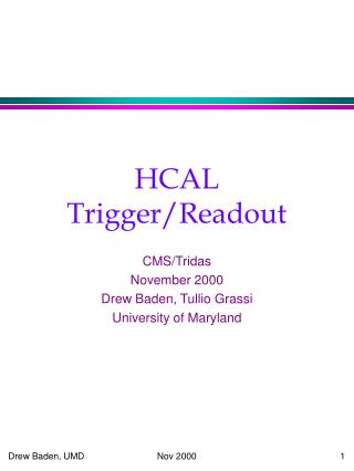
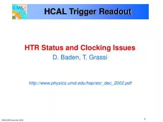
HCAL TPG and Readout. CMS HCAL Readout Status CERN Drew Baden University of Maryland March 2002 http://macdrew.physics.umd.edu/cms/ see also: http://tgrassi.home.cern.ch/~tgrassi/hcal/. Front End Electronics. TTC fiber. Gbit Ethernet @ 1.6 Gb/s. F a n O u t. B I T 3. H

E N D
HCAL TPG and Readout CMS HCAL Readout Status CERN Drew Baden University of Maryland March 2002 http://macdrew.physics.umd.edu/cms/ see also: http://tgrassi.home.cern.ch/~tgrassi/hcal/ HCAL TriDAS
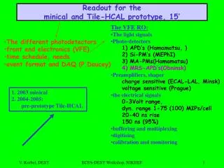
Front End Electronics TTC fiber Gbit Ethernet @ 1.6 Gb/s F a n O u t B I T 3 H TR H T R H T R H T R D C C (s) ... 20 m Copper Links 1 Gb/s DAQ Calorimeter Regional Trigger Readout Crate Changes • Outside world – slow monitoring, controls…. • Bit3 PCI/VME interface • Known quantity • 3U Rack Computer • Dual processor DELL, fast PCI bus • Chris Tully to take responsibility • I’m keeping track of M&S for operations • Not yet added to WBS (I think….) • UIC/HRC replaced by TTC/Clock Fanout • “HRC” did some of the above • Clock fanout is critical for VME crate functions • Fanout to all HTRs • Fewer HTR/crate • Mapping considerations • Dual-width DCC considerations • Not yet settled. I don’t like it…but we’ll see… HCAL TriDAS
HCALTRIGGERandREADOUTCard • No functional changes since Dec-2001 • I/O on front panel: • Inputs: Raw data: • 16 digital serial fibers from QIE, 3 HCAL channels per fiber = 48 HCAL channels • Inputs: Timing (clock, orbit marker, etc.) • PECL • Outputs: DAQ data output to DCC • Two connector running LVDS • TPG (Trigger Primitive Generator, HCAL Tower info to L1) via P2/P3 • Use aux card to hold Tx daughterboards • Via shielded twisted pair/Vitesse • FPGA logic implements: • Level 1 Path: • Trigger primitive preparation • Transmission to Level 1 • Level 2/DAQ Path: • Buffering for Level 1 Decision • No filtering or crossing determination necessary • Transmission to DCC for Level 2/DAQ readout HCAL TriDAS
Demonstrator Status • Demonstrator • 6U HTR, Front-end emulator • Data, LHC structure, CLOCK • 800 Mbps HP G-Links works like a champ • Dual LCs • This system is working. FEE sends clock to HTR, bypasses TTC • HCAL FNAL source calibration studies in progress • Backup boards for ’02 testbeam • Decision taken 3/02 on this (more…) • Anticipate we will abandon this card for testbeam • DCC full 9U implementation • FEE HTR DCC S-Link CPU working • Will NOT demonstrate HTR firmware functionality as planned • Move to 1.6 Gbps costs engineering time • Firmware under development now 6U HTR Demonstrator 6U FEE HCAL TriDAS
HTR “Dense” Scheme Throughput: 17 Gb/s Latency: + 2 TCK DeS DeS DeS P1 FPGA Xilinx Vertex-2 SLB -PMC OPTICAL Rx (8 LC) DeS 8 FE fibers 24 QIE-ch’s DeS SLB -PMC DeS P2 LVDS Tx DeS DeS to DCC SLB -PMC Trigger output 48 Trigger Towers DeS DeS SLB -PMC DeS FPGA Xilinx Vertex-2 DeS OPTICAL Rx (8 LC) SLB -PMC 8 FE fibers 24 QIE-ch’s DeS P3 DeS SLB -PMC to DCC LVDS Tx DeS DeS 9U Board HCAL TriDAS
“Dense” HTR • Dense (48 channel) scheme is now the baseline • Money • Fewer boards! • Programmable logic vs. hardware • Avoid hardware MUXs • Maintain synchronicity • Single FPGA per 8 channels • Both L1/TPG and L1A/DCC processing • Next generation FPGAs will have deserializers built in • Xilinx Vertex-2 PRO and Altera Stratix announced • Saves $500/board $100k • ~20 connections to deserializer reduced to 1 connection at 1.6 GHz • Single clock would serve 8 deserializers • Probably won’t get to have any of these chips until summer 02….schedule may not permit • We will keep our eye on this • 48 channels x 18 HTR x LVDS Tx to DCC exceeds DCC input bandwidth • So, need 2 DCC/crate (but fewer crates) HCAL TriDAS
Prototype Status FPGA+8 deserializers • TPG transmission changed • From SLB mezzanine cards to Backplane aux card • Solves mechanical problems concerning the large cables to Wesley • 1.6 GHz link • Wider traces, improved ground planes, power filtering, etc. • Deserializer RefClock fanout • TTC daughterboard changed to TTC ASIC • Fixed TI deserializer footprint problem • Clocking fixes • Next iteration estimate • Submit in 2 weeks • Stuffed and returned • by April 1 VME FPGA Out to DCC TTC and Clock distribution Dual LC Fiber Connector OLD DESIGN HCAL TriDAS
Current Hardware Status HTR 2 deSerializers Dual LC (Stratos) Receivers • 1.6 GHz link is the hardest part • Made a “LinkOnly” board • 2 dual LCs feeding 4 TI deserializers • TI TLK2501 TRANSCEIVER • 8B/10B decoding • 2.5Volts • 80MHz frame clock • 20 bits/frame • Internal use only • This board works. • We “know” how to do the link now • Did not test the tracker NGK option NGK “Tracker” Dual LC (Stratos) Transceiver HCAL TriDAS
HTR Issues • Optical link • Stratus LC’s work well, available, not very expensive, probably will get cheaper. • “Tracker solution”? We think no…this option appears to be dead. • NGK/Optobahn not responsive • Time scales for HTR is this summer • Tracker group has kept us at arms length with respect to vendors • Anticipate much ado about getting quotes and signing orders – schedule risk is too great • Savings is approximately $50/channel ($150k overall) • Expect LC’s to get cheaper…will the NGK? • Clocking • Jitter requirements are surprising – refclk needs to be 80MHz ± ~30kHz to lock and stay locked. • This is because we are using a Transceiver, not a Receiver • TI does not have a Receiver – this is Gigabit ethernet, so it’s meant for 2-way • We can implement in 2 ways • Onboard crystal • PECL clock fanout • Will have both for next iteration, board that will be in the testbeam summer ’02 HCAL TriDAS
HTR Board TTC Fanout Board SLB Board deserializers TTCrx 1 to 8 Fanout TTC MUX 80 MHz LVPECL Crystal TTC PECL Fanouts to HTRs 1 to 8 Fanout 1 2 Fanout Clock/BC0 80 MHz 40 MHz Clock/2 HTR Clocking • TTC provides input clock for the VME crate modules. • Clocks needed: • DCC not critical • HTR: • Deserializers (16) need 80MHz clock with ~40ps pkpk jitter • TPG transmission needs 40MHz clock with ~100ps pkpk jitter • Pipeline needs 40MHz clock synchronous with data transmission • Options – eliminate: • 80MHz crystal (eliminates 1 Mux) • TTC Fanout Board clock to deserializers (eliminates 1 2 Fanout and 1 Mux) • We will see what we learn at the Testbeam ‘02 HCAL TriDAS
HTR Schedule Production Phase Production Checkout 3-6 FTE month FPGA coding ongoing • Testbeam Phase • Next Checkout: 3 months • Fix problems: 0.5 months • Next checkout if needed: 1 month • Production Phase • Prep for next pre-production run: 1 month • Checkout for production prototype: 1 month • Production checkout: 3-6 months • FPGA coding: 6 months ? • Total: 1.5 FTE years, around $180k • Integration: ongoing…difficult to say Prepare Prod’n Prototype 1 FTE month April 02 Prototype 4/1/02 Production Prototype May 02 Production Run Fall 02 Checkout Prod’n Prototype 1 FTE month Jun-Aug 02 Checkout 2-3 FTE months April 02 In parallel Next iteration requires less checkout time…. May 02 OK? Fix 2 FTE weeks Testbeam Run May/June 02 Cards at CERN July 1 at latest Testbeam Phase HCAL TriDAS
Test Beam Jun-Sep Done FNAL source calib. Slice Test I Current Project Timeline 2000 2001 2002 2003 2004 Demonstrator Project 1.6 GHz Link Pre-Prod Production Begins between March and Sept 2003 Installation STILL SOME UNCERTAINTIES… • Vertex-2 PRO or Altera Stratix • Global clocking scheme • Clock jitter HCAL TriDAS
DATACONCENTRATORCARD Motherboard/daughterboard design: • VME motherboard to accommodate • PCI interfaces (to PMC and PC-MIP) • VME interface • In production (all parts in house) • PC-MIP cards for data input • 3 LVDS inputs per card • 6 cards per DCC (= 18 inputs) • Engineering R&D courtesy of D • In production (purchasing underway) • Logic mezzanine card for • Event Building, Monitoring, Error-checking • S-Link64 output to TPG/DCC and DAQ • Fast busy, overflow to TTS • Giant Xilinx Vertex-2 1000 (XC2V1000) • Transmission to L2/DAQ via S-Link PCI Interfaces P2 P0 P1 6 PC-MIP mezzanine cards - 3 LVDS Rx per card Data from 18 HTR cards PMC Logic Board Buffers 1000 Events TTCrx TPG DCC DAQ “Fast” (Busy, etc) HCAL TriDAS
Current Status DCC Motherboard • VME Motherboard • Production starting • 5 prototypes in hand for CMS. • All production parts bought • PCB / Assembly order ~ May ‘02 HCAL TriDAS
Current Status DCC Logic Board and LRBs • PC-MIP Link Receiver • Design approved except for changeto RJ-45 connector for links • Final prototype PCBs on orderProduction parts on order • Production to start ~ June ‘02 • Logic Board – final prototype • Decisions about S-Link Data Width / Card location • Expect final PCB design lateCY 2002 • Production in early 2003; driven by finaldecisions about functionality HCAL TriDAS
HCALTIMINGFANOUTModule • Fanout of TTC info: • Both TTC channels fanout to each HTR and DCC • Separate fanout of clock/BC0 for TPG synchronization • “daSilva” scheme • Single width VME module HCAL TriDAS
Testbeam Clocking • The only sane thing is to run the entire setup from a single high purity clock • TTC input is single-ended LIMO. • Source of “our clock” had better be clean. • Chris will make us a 6U VME board • 35MHz crystal, care taken on transmitter. Will be in same VME crate as TTC • Can also put 30MHz, 37MHz, 40MHz…jump selected for playing around • We will have the same high quality clock for Tx and Rx • HTR will have Crystals as a backup just in case…. Front End Fiber Data, QIE HTR TTC System Fiber “Our Clock” Single-ended Readout Crate HCAL TriDAS
Cost to Completion – M&S • Not much change in DCC, VME Rack, VME Crate unit costs • HTR cost increases by ~7% • $320/board due to: • $100/board due to quality requirements on traces (need constant impedance lines) • $100/board for clock circuitry (Xtal, PECL stuff, etc.) • $120/board for LC’s (old estimate was based on quads, but we’re going with duals) • Addition of HTR backplane card to support 48 channel HTR – net savings • Cost decreases will surely come, but we don’t know now. • LC’s will only go down in price • TI deserializers are transceivers, receivers will be cheaper, TI will have to compete…FPGAs w/deserializers…. • HRC replaced by TTC Fanout + Bit3 + Crate CPU • Mapping really constrains us • Some HTR will not be full of SLBs • Still requires 1 SLB transition card per HTR • Some crates will not be full of HTRs • Original cost had up to 18 HTR/crate, now it’s around 14 • Results in a few more crates than 9/01 cost estimate HCAL TriDAS
Cost to Completion – M&S (cont) HCAL TriDAS
HTR Itemized Cost (Appendix) • Costs as of April 2001…. • 12 fibers/card, 3 channels/fiber Lehman 01 slide 4x$750=$3k 2x$1.2k=$2.4k Tullio doesn’t believe it. Up to $500 Tullio doesn’t believe it. Up to $400 $640 for 16 dual LC’s 8 vs. $580 for 16 TTC/clock circuitry since then X2 = $5420 v. $5120 without reductions HCAL TriDAS
Additional M&S Costs • Test stands never accounted for • $29k/crate total • Proposal calls for 3 test stands - $87k total • 1 @ FNAL • 1 @ UMD/BU/Princeton • 1 @ CERN • This one used for testbeam and then moved to USCMS electronics area • “EM Trigger” • Rohlf estimates 1 crate ($5.5k), 2DCCs ($10k), 12 HTR ($62k) • If we need additional Bit3 and CPU, it’s another $6.7k • Total would be $84k • Testbeam • We will be producing HTRs that may, or may not, be final versions. • If so, no problem. If not, additional costs • Estimate around 6 HTR including 2 spares, comes to around $40k HCAL TriDAS
Cost to Complete – Effort BU/UIC • Difficult to predict • UMD: 1.5 FTE years (previous slide) • BU 1.5 FTE years • Testbeam extra work: 3 FTE months • Finish DCC prototype (FPGA code): 4 FTE months • DCC “final prototype”: 6 FTE months • SLINK64, 2-slot or Transition board… • Test engineering: 2 FTE months • “UIC” • 1 FTE engineer, should be finished with TTC fanout by Fall 02 • FNAL might want to keep him around to help with system clock issues HCAL TriDAS
Project Status Summary • HTR (Maryland): • 6U Demonstrator done • Testbeam Effort • OK if no disasters • But…integration is going to be a big effort and will interfere with Production effort • Production Effort • FPGA coding ongoing • Will work on HTR in parallel w/testbeam effort • TTC fanout • First board assembled and tested • Next iteration underway - Will be ok for testbeam • Crate CPU issues • Chris Tully is playing with Bit3 and DELL 3U rack mounted dual CPU • DCC • 9U Motherboard done., PCI meets 33MHz spec, Production run beginning • Link Receiver Cards - Built, tested, done. • Logic board • Underway. Only issues are FPGA Coding, Backplane card vs. double-width HCAL TriDAS