Download
1 / 21
210 likes | 346 Views
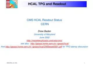
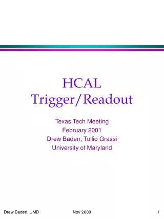
HCAL Trigger Readout. HTR Status and Clocking Issues D. Baden, T. Grassi http://www.physics.umd.edu/hep/esr_dec_2002.pdf. SBS. CLK. D C C. CAL REGIONAL TRIGGER. H T R. H T R. H T R. 16 bits @ 80 MHz. TTC. 32 bits @ 40 MHz. QIE. CCA. GOL. QIE. QIE. CCA. QIE. GOL.

E N D
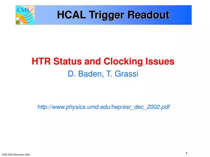
HCAL Trigger Readout • HTR Status and Clocking Issues • D. Baden, T. Grassi • http://www.physics.umd.edu/hep/esr_dec_2002.pdf
SBS CLK D C C CAL REGIONAL TRIGGER H T R H T R H T R 16 bits @ 80 MHz TTC 32 bits @ 40 MHz QIE CCA GOL QIE QIE CCA QIE GOL QIE CCA QIE FE/DAQ Electronics S-Link: 64 bits @ 25 MHz Trigger Primitives READ-OUT Crate Rack CPU 12 HTRs per Readout Crate, 2 DCC FRONT-END RBX Readout Box (On detector) HPD Shield Wall Fibers at 1.6 Gb/s 3 QIE-channels per fiber FE MODULE
HTR Principal Functions • Receive front-end data for physics running • Synchronize optical links • Data validation and linearization • Form TPG’s and transmit to Level 1 at 40 MHz • Pipeline data, wait for Level 1 accept • Upon receiving L1A: • Zero suppress, format, transmit to the concentrator (no filtering) • Handle DAQ synchronization issues (if any) • Calibration processing and buffering of: • Radioactive source calibration data • Laser/LED calibration data • Support a VME data spy monitoring
“BIT3” board Slow monitoring over VME Commercial VME/PCI Interface to CPU FanOut board Takes TTC stream in Clone and Fanout timing signals HTR (HCALTrigger and Readout) board Spy output over VME FE-Fiber input TPG output (SLBs) to CRT DAQ/TP Data output to DCC DCC (Data Concentrator Card) board Input from HTRs Spy output Output to DAQ Readout VME Crate Front End Electronics TTC fiber Fiber 1.6 Gb/s F a n O u t VME CRATE B I T 3 H TR H T R H T R H T R D C C ... D C C 20m Copper 1.2 Gb/s DAQ Calorimeter Regional Trigger
“Old” HTR Design (Summer 2002) • Board organized around 2 identical sets of circuitry: • Optical inputs • 1.6 GHz, 8B/10B frames, 3ch/link • Dual LC detectors and drivers • TI TLK2501 Deserializers • Crystal RefClk • TTC 80MHz backup • Xilinx Virtex FPGA XCV1000E • 24 channels each • TPG signals • Sent to SLB over backplane, LVDS • SLBs mounted 6 to a transition board • Level 1 accept output to DCC • LVDS output • VME • Altera FPGA and firmware OLD DESIGN
HTR Functional Experience • What was tested: • VME fully tested and working • Some changes necessary to conform to CMS VME standards • Optical links and synchronization • No indication of any problems. Big success here – was a real worry • LVDS to DCC • Tested, working (Will change cable/connector to Cat 6/RJ45) • Fanout of timing signals on two Cat5 cables • Plan to change to a single Cat6 or Cat7 cable (very low cross-talk) • Firmware – full tests of: • Pipeline and L1A triggering capability • In-line histogramming for source calibration • TTCrx • Not working at all (4 bad on 4 tested). • What was not tested: Anything to do with TPG
HTR Board Experience • Produced ~12 boards • Several bare boards were delivered warped • Many opens under FPGA after assembly (~9 boards) • Some fixed after reflow (a few) • Some worse after reflow (shorts) • X-rayed a few boards, sometimes inconclusive • Some opens on VME side • Non BGA FPGA, indicates bad vias • Few other various open circuits • Finally got ~8 boards to “work” • Questionable reliability
Modifications • Change board from using white-tin to gold traces • This process was sold to us by the board maker. Our mistake. • Used only for very high volume, cost competitive products, very difficult and expensive to control. • Gold is flatter and not very much more expensive (~$50/board), better for FPGAs • Change assembly house • Insufficient Quality Control on current assembler – they are fired. • We visited 2 high-end assemblers • Modern Machines • Step up and step down oven temp control. • In-line X-ray for BGA QC • Manufacturability Review • Add stiffeners to HTRS • Flexability of 9U VME boards was underestimated • Worry: fine-line BGA (FBGA) can pop connections
Modifications (cont) • Change from FBGA to BGA • FBGA 1.0mm pitch, change to BGA 1.27mm pitch • No additional expense, plenty of available real estate, no need to push • We are just being very conservative here • JTAG capabilities added • Will help with debugging • By making these changes… • We have profited from the summer • We have reduced our production risk considerably
HTR Design Changes • SLB transition board issues: • Worries about so many LVDS signals over backplane for old design • Routing is too complicated • Many signals going to same backplane location • Requires multi-layer routing with many vias • TPG cables very thick • Mechanical issues are very worrisome • SLB changes needed (e.g. height reduced after ECAL redesign…) • Solution: move SLB’s to HTR motherboard • Benefits: • Mechanically attach SLB’s to HTR front panel for mechanical stability • Eases routing requirements, reduces board and assembly risks, cheaper too • Change from Xilinx VirtexE to Virtex2 • More resources, block ram, hardware multipliers • Big cost reduction (save $180k) • More modern chip for long-term maintenance • Clock synchronization • Decouple “80MHz” crystal from FPGA system clock • Will allow us to use crystal to maintain synchronization of serdes • This gives us 2 solutions for our “40ps” jitter requirement issue
LVDS LVDS LC LC LC LC LC LC LC LC SLB SLB SLB SLB SLB SLB New HTR Conceptual Design Fibers 8-way P1 TI TI 8-way TI FPGA Xilinx XC2V to DCC VME FPGA TI TI P2 TI TI TI TI TI to Level 1 Cal Trigger TI FPGA Xilinx XC2V TI TI No P3! TI TI TI TTC from Fanout RJ45
TTCrx Clocking Schematic • Start with Fanout card • TTCrx Maryland mezzanine card or CERN TTCrm daughterboard • QPLL • Fanout on Cat6/7 quad twisted pair TTC, BC0, 40MHz, 80MHz • In HTR: • Send TTC signal to TTCrx mezzanine board, access to all TTC signals • Send 80MHz clean clock (cleaned by QPLL) to mux • Select 80MHz clean clock OR crystal to TI deserializers Cat 6/7 quad cable (allows PECL) TTC Fanout Board 80 MHz LVPECL Crystal FPGA SLB TI (16) TTC 80MHz 1 to 8 Fanout QPLL SLB BC0 80MHz SLB BC0 BC0 40MHz 1 to 8 Fanout SLB SLB 80 MHz 1 to 8 Fanout 40MHz SLB 40 MHz TTC mezz TTC broadcast bus TTC Single width VME
TTC BC0 CC40CC80 HCAL TRIDas Clock Scheme Fanout Card QPLL TTCrx Cat6/7 RJ45 4 twisted pair… (‘CC’ means Clean Clock) TTC TTCMezz TTC broadcast, L1A, BCR, EVR, CLK40 RJ45 Xilinx CC80 CC40 SLB HTR Board BC0
FPGA TTCrx (or daughter card) PCK953 LVPECL- to-LVTTL Fanout (top layer) PCK953 LVPECL- to-LVTTL Fanout (top layer) PECL fanout PECL fanout QPLL MC100LVEL37 80.0789 MHz 3.3V crystal Diff. PECL CK CK CK/2 CK/2 TTC daughter card IN IN_b Notes: SLBs require fanout of CLK40, BC0. FE-link possibly requires CLK80. PECL fanout was tested in TB2002. One Cat6E cable (low x-talk) replaces the 2 Cat5 cables used in TB2002. TTC and BC0 remain LVDS as in Weiming’s board. HTR needs Broadcast bus, BCntRes and L1A: from TTCrx if we get it to work, otherwise we have to fan them out. Fanout – HTR scheme TTC fiber Fanout buffer O/E TTC TTC LVDS TTC DS90LV001 Low-jitter Fanout x 15 ~Fifteen RJ45 connectors Brdcst<7:2>, BrcstStr, L1A, BCntRes to xilinx and SLBs e.g. DS90LV110 RJ45 TTC LVDS Fanout x 8 .. .. .. .. Diff. to 6 SLBs Single-end to 2 xilinx .. .. .. .. RX_BC0 LVDS Brdcst<7:2>, BrcstStr LVDS BC0 Cat6E or Cat7 cable Q1 Q2 Q3 Q4 Q5 Q6 Q7 Q8 CLK40 3.3V-PECL To 6 SLBs Diff. to 2 Xilinx + termin. CLK40 LVDS 2 Test Points for CLK40 and BC0 .. .. 8 clks to TLKs CLK80 LVDS MC100LVE310 3.3V PECL NB100LVEP221 is LVDS compatible AN1568/D Fig 11 Onsemi.com CLK80 3.3V-PECL …….. …….. 15 Cables & Connectors tbd Fanout x 15 Brdcst<7:2>, BrcstStr, BCntRes, L1A …….. …….. …….. …….. CMOS LVDS or diff PECL 15 connectors on bottom layer ? Fanout Board 8 clks to TLKs + TPs HTR 9U Front-panel space = 325 mm ; => space per connector ~ 21.5 mm Tullio Grassi <tullio@physics.umd.edu>
TTCrx Mezzanine card • Very simple card: • 2 PMC connectors • TTCrx chip • TTC signal driver on motherboard • Will be sent out for prototype next week • Used by HTR, DCC, and Fanout cards
TTC Distribution – Fanout Card • Currently HCAL has 6 TTC partitions: • Each partition requires TTCvi and TTCex • Each HCAL VME crate will have a single TTCrx receiving data directly from TTCex in a single VME card (Fanout Card) • Fanout TTC signal to HTR mezzanine card with TTCrx chip • Use quad twisted pair CAT6/7 cable allows PECL fanout • TTC raw, BC0, 40MHz clean, 80MHz clean fanout • Cost savings and simplification • TTC monitoring by Fanout card over VME • Count resets, etc…
Random Latency Issue • Texas Instruments TLK2501 Serdes • Run with 80MHz frame clock – 20 bits/frame, 1.6GHz bit clock • 625ps bit time • Latency from data sheet: • ~20ns variation (overall latency between 47 and 67ns) • Fiber to fiber alignment could cross a 40MHz bucket boundary. • How to fix? • SLB “knows” this latency – we will read it out after each reset • HCAL LED fast rise time • Can pulse during abort gap and align channels • Requires LED pulsing alignment • FE will send BC0 signal on all fibers • Will measure this alleged latency with new HTR boards
TPG Alignment • TPG alignment performed in SLB • Necessary: All HTRs will send common BC0 to SLB’s within each of 16 VME crates • Calibration procedure to be performed for crate-crate alignment • Initial alignment with LEDs, laser, etc. • Final alignment with LHC first beam data • Use “1-bucket” running to check everything • This will ensure successful alignment
DAQ Alignment • DAQ data must also be aligned • Must know L1A bucket for zero suppression • Only if we will do ZSP on 1 or 2 HCAL channels centered on L1A bucket • If ZSP done with sum over 5 channels, then this alignment is not critical • Solution: discussed in previous slide • Read from SLB • FE sending known ID after with fixed offset relative to BC0 during abort gap • Comparison of the two for error checking • DAQ check on BC0 in DCC for alignment • Will send BC0, BCN, and EVN with the data to DAQ
MISC Errors • What happens if DCC finds mismatch in EVN? • DCC will then issue resynch request to aTTS system • Details not yet defined but is fully programmable • Fiber Link/synchronization errors (GOL/TI) • Work out protocols to inform DCC • Reset requests to aTTS as well • FE Clock/GOL PLL link errors • If GOL loses synch, then transmitter will send out IDLE characters • IDLE characters are illegal in a pipelined system! • HTR will trap on IDLE as a signal that FE/GOL is having trouble