Download
1 / 1
10 likes | 119 Views
Buffer Link Design in a Network-on-Chip Andrés Arocho 1,2 , Justin Frye 2 , Lei Wang 2 and EJ Kim 2 1 Department of Computer and Electrical Engineering , University of Puerto Rico, Mayagüez Campus 2 Department of Computer Science and Engineering, Texas A&M University. Performance.

E N D
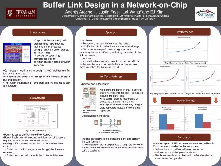
Buffer Link Design in a Network-on-Chip Andrés Arocho1,2, Justin Frye2, Lei Wang2 and EJ Kim2 1Department of Computer and Electrical Engineering , University of Puerto Rico, Mayagüez Campus 2Department of Computer Science and Engineering, Texas A&M University Performance Introduction Approach • Chip Multi-Processors (CMP) architectures have become mainstream for processor designs. (Intel 80-core Teraflop, Tilera 64-core) • Network-On-Chip (NoC) provides an efficient communication method for CMP systems. • Low Power: • - Remove some input buffers from the router. • - Modify the links to make them work as extra storage. • - We minimize the performance degradation of removing the input buffers by activating the buffers in the link as needed. • Low area: • - A considerable amount of transistors are saved in the router area by removing input buffers as they occupy more area than the buffers in the link. Original Scheme vs. Buffer Link Design (No saved power or area) • Our research work aims to design a NoC architecture for low power and area. • We revisit the buffer link design in the context of static buffer allocation. • The buffer link design is compared with the original router architecture. Buffer Link design • Modifications in the router: • To control the buffer in links, a control block insertion into the router is made to activate the buffer link. • The control block is responsible of activating the buffer in the links. • Storage of packets is done by using tri-state repeaters instead of the original repeaters. • Traditional high performance are less practical. • Shrinking size of NoC technology. • Power dissipation is a key constraint. Original 8 input buff vs. B.L.D 7 input buff, 3 buff link Original 10 input buff vs. B.L.D 8 input buff, 8 buff link Background Power Savings Fig 2. Modifications to router. • Modifications in the links: Fig 1. Basic Router Architecture Fig 3. Modification in the links. • Router is based on Wormhole Flow Control. • Router implements the routing and flow control functions required to forward packets to destination. • Adding buffers to a router results in more efficient flow control. • - Buffers account for major power budget, but they are necessary. • - Buffers occupy major area in the router architecture. Conclusions • Adding transistors to the repeaters in the link perform • the dual-function • The congestion signal propagates through the buffers in the link when the downstream router does not have more buffers available. • We save up to 18.38% of power consumption, with only 4% of performance drop in the worst case. • Reduce the input buffers in the routers saves considerable amount of power and area. • Simulation results show that static buffer allocation is • an attractive configuration.