Download
1 / 24
240 likes | 389 Views
Introduction : ECAL Physic prototype. Mechanic : Slab & Alveolar structure Rotating system Final structure (full detector) PCB : production Spare Proto. Completion Silicon sensors : Matrix specification Characterization Set-Up Wafer production Czech Russian Other ….

E N D
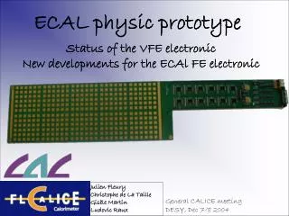
Introduction : ECAL Physic prototype. Mechanic : Slab & Alveolar structure Rotating system Final structure (full detector) PCB : production Spare Proto. Completion Silicon sensors : Matrix specification Characterization Set-Up Wafer production Czech Russian Other… R&D on Si sensors AC coupling Smaller pixel size Slow control : Elect. Power supplies Wafer Power supply Temp. monitoring Cosmic Calibration : Test Structure 1 + DAQ (UK) DESY cosmic calibration Beam Test : DESY CERN Conclusion Calice ECAL Prototype Status
Multi-layer (30) W-Si Prototype : 3 independent C-Walveolar structures according to the thickness of tungsten plates (1.4, 2.8 and 4.2 mm) 30detector slabs which are slid into central and bottom cells of each structure Active zone : 33 wafers 30 layers Introduction : prototypes for test beam Design and Prod : LLR Integration : LLR Structure 2.8 (2×1.4mm of W plates) Structure 1.4 (1.4mm of W plates) Structure 4.6 (3×1.4mm of W plates) ACTIVE ZONE (18×18 cm2) 3 structures W-CFi (1,2,3 x1.4mm) 30 « detteur slabs » Dimension 200x360x360 mm 9720 channels in the proto. 270 Wafers Si with 6×6 pads (10×10 mm2)
Composite Structures • Design and fabricationof alveolar structureswith associated moulds -Alveolar structures:3/ 3 • Design and fabricationof 30 type H structures with associated moulds - H with W = 1.4 mm : 10/ 10 - H with W = 2.8 mm : 10/ 10 - H with W = 4.2 mm : 10/ 10 Alveolar structure mould : Structure H mould : Alveolar structure Tungsten plates Type H structure
Gluing wafers & Slab assembly • Assembly mould • Validation of each steps to glue wafers on PCB : - Glue : EPO-TEK E4110 - OK - Dispensing system- OK - Placing manually wafers - OK - Aluminium foil process - OK - Polymerisation : 8h@40°C - OK • Production of PCB : (2 days / PCB) • Validation of the Slab assemblyprocess : - Bending tool of shielding - OK - Assembly mould- OK - Polymerisation : 8h@40°C - OK • Production of Detector SLAB : (1 day / SLAB) - Central SLAB : 07 / 15 - Bottom SLAB : 00 / 15 • Placing wafers on PCB waiting for matrices since February 2005 !
Mechanic : Rotating system & Final Structure • Rotating system : • Final structure (whole ECAL) : calculation in finite element of the final structure in progress (constraint, deformation …)
2 calibration switches chips 6 calibration channels per chip 18 diodes per calibration channel 6 active wafers Made of 36 silicon PIN diodes 216 channels per board Each diode is a 1cm² square Line buffers To DAQ part Differential 12 FLC_PHY3 front-end chip 18 channels per chip 13 bit dynamic range Front-end PCB 14 layers 2.1 mm thick Made in korea
Production : PCB + Chip In February 2005 : Mainly due to assembly
Production : PCB + Chip Today : Spare : 20 more PCB delivered (Korea) 10 for central part 5(L) + 5(R) for the bottom part Ready in December.
Production : PCB + Chip + Wafer : Slab Full PCB : 15 + (1) Half PCB Right : 1 + (1) Half PCB Left : 0 Full Slab : 7 Half Slab : 0
Physic prototype : completion We have ordered (end march 2005) 100 matrices from INP in Russia in order to complete the central part of the prototype. The first 24 were delivered at EP in mid September.
62 mm 62 mm Silicon sensors : Matrices 4” High resistive wafer : 5 Kcm Thickness : 525 microns 3 % Tile side : 62.0 + 0.0 - 0.1 mm Guard ring In Silicone ~80 e-h pairs / micron 42000 e- /MiP Capacitance : ~21 pF (one pixel) Leakage current @ 200 V : < 300 nA (Full matrix) Full depletion bias : ~150 V Nominal operating bias : 200 V Break down voltage : > 400 V Si Wafer :6×6 pads of detection (10×10 mm2) • Important point : manufacturing must be as simple as possible to be near of what could be the real production for full scale detector in order to : • Keep lower price (a minimum of step during processing) • Low rate of rejected processed wafer • good reliability and large robustness • Wafers passivation Compatible with a thermal cooking at 40° for 12H, while gluing the pads for electrical contact with the glue EPOTEK E4-110 polytec (conductive glue with silver)
Silicon Sensors : characterization set-up • I(V) Leakage & Breakdown • I(t) aging • 36 pixels must be polarized Conductive Foam
Silicon Sensors : new characterization set-up • new system with 36 contacts done with points gone up on springs allowing us to perform : • I-V curve • C-V curve • C-V meter • Pico ammeter • High voltage power supply • temperature monitoring • humidity monitoring
Silicon Sensors : Production February 2005 Pb after gluing… ~76 %
Silicon Sensors : Czech Production • April 2005 : in collaboration with people from Prague • Different chemical passivation • Different gluing protocol (Temp., Time and glue) results not very conclusive wafers already manufactured cannot be recovered • August2005 : • 10 new processed wafers from ONsemi • Before gluing : stable • After gluing : • Leakage increase • Vbr seems stable
Silicon Sensors : New Russian Production I-V curves 24 matrices delivered at EP in mid September C-V curves Leakage, Breakdown : 4 to 5 bad Depletion voltage : 6 bad (Not all measured) At best only 62 % are good !
Silicon Sensors (end) • Looking for new producer : • Korean will produce 50 sensors (December) • Close contact with other producers • Decrease the pixel size 3x3 mm2 • Mechanical test with the glue dot of 1 mm in diam. seems possible • Electrical test soon (resistivity) • AC versus DC coupling We have ordered 500 raw wafers (high resistivity) !
Calibration Cosmic test bench • Calibration of the slab must be done before test beam • At EP we have just single slab DAQ just go no go test after slab assembly • About 10 days to achieve 1% • Must be done structure by structure. • Need VME DAQ • End of December 2004 at EP : • One structure (5 slabs) • 10 days ~ 1 million of cosmic events Calibration into cosmic planned with DESY from November 15, 2005 Calibration : 1%
Slow Control During test beam in Februaryno slow control we need ! • New switching power supplies for low voltage (-5, +5 and -6V) with GPIB • High voltage power supply (200V) with GPIB • GPIB to USB interface (from NI) • USB Long Distance Repeater • PC + software under construction + socket to UK DAQ • We need also to add temperature monitoring
Test beam DESY (I) • February 2005 Test : • Ecal • Structure 1 and 2 • 7 Slabs, 14 layers • 84 matrices 3024 pixels • Motorized XY support • Drift chamber (200 m resolution) • VME DAQ • ~ 13 full days of run Great thanks you to Norbert Meyners and all AHCAL people for their help.
Test beam DESY (II) • February 2006 Test : • Ecal • Structure 1,2 and 3 • 15 Slabs, 30 layers • 180 matrices 6480 pixels • Motorized XY support • Drift chamber (200 m resolution) • Slow control (power supplies and temperature monitoring) • VME DAQ • ~ 15 full days of run Great thanks you to Norbert Meyners and all AHCAL people for their help.
Test beam CERN • Spring 2006 Test : • Ecal • Structure 1,2 and 3 • 15 Slabs central part • 15 Slabs bottom part • 270 matrices 9720 pixels • Motorized XY support • Beam hodoscope?? • Slow control • VME DAQ • ~ xx full days of run Picture soon !! Great thanks you to Norbert XXXXXX and all XXXXX people for their help.
Summary • Si sensors • Improvement of the characterization set-up • Czech sensors in progress but still some problems • Russian new production : rate is decreasing • Looking for other producers • Test beam • Calibration mandatory with cosmic and VME DAQ • DESY test in February with 30 layers !! • Slow control • Improvement of the mechanical support • CERN test : full completion of the prototype ? • Need some spare