Download
1 / 17
170 likes | 377 Views
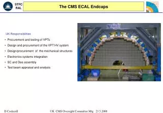
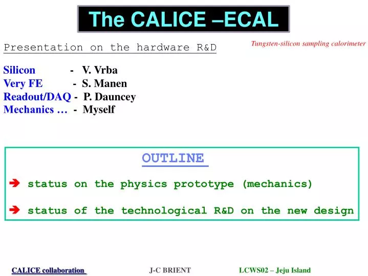
The CALICE –ECAL. Tungsten-silicon sampling calorimeter. Presentation on the hardware R&D. Silicon - V. Vrba Very FE - S. Manen Readout/DAQ - P. Dauncey Mechanics … - Myself. OUTLINE status on the physics prototype (mechanics)

E N D
The CALICE –ECAL Tungsten-silicon sampling calorimeter Presentation on the hardware R&D Silicon - V. Vrba Very FE - S. Manen Readout/DAQ - P. Dauncey Mechanics … - Myself OUTLINE status on the physics prototype (mechanics) status of the technological R&D on the new design
The mechanics for the physics prototype Tungsten metrology Detector slab design W-Carbon fiber structure The LLR mechanics groupparticipating M.Anduze, A.Busata, P.Maritaz, D.Pineihro, P.Poileux,etc…
1st structure (1.4mm of W plates) 2nd structure (2×1.4mm of W plates) 3rd structure (3×1.4mm of W plates) HCAL VME ECAL Electronics 370 mm 370 mm 180 mm Beam monitoring Detector slab Movable table Silicon wafer Movable table Physics Prototype – global presentation from Marc Anduze (LLR) The CALICE-ECAL physics prototype beam
Tungsten metrology The first 3 tungsten plates measured at LLR It confirms the good quality of the plates As measured at IHEP and ITEP. Assuming no strong Geometrical correlation Like for the first 3 plates Marginal impact on the energy resolution for single particle* * Following MOKKA and GEANT4
Detector slab schematic view • Prototype configuration : using PCB solution + external Frond End Shielding Silicon wafer PCB Front End electronics (CFi / W) structure type H
Carbon fiber Tungsten 1.4 mm thick Structure W-Cfi 5 alveoli (10 layers) Structure type H Piece of the first structure
Structure type H with its aluminum shielding
Summary on the ECAL prototype DONE The production of a sample of 40 tungsten platesstarts. it corresponds to the first technological test and first stack of prototype Production of the final set of masks for the silicon wafersand successful processing of the first 25 silicon wafers (DC coupled) at MSU The design of the front-end chipis fixed. First batch for test in September. Fall 2002 Processing and test of about 100 silicon wafers(PRAGUE, MSU, LLR) Final submission of theVFE chip for the prototype(LAL) Construction of the first 1/3 of the W-CFi structure of the prototype(LLR)
R&D on the new design of the full scale detector A design with electronics inside detector AC coupling elements ? Thermal contact Aluminium 1.3 mm Cooling tube Cooling tube VFE chip powerline command line signal out 1.0 mm PCB Pad 0.5 mm Silicon wafer Gluing for electrical contact
Advantages and drawbacks Advantages A priori, all processes are uncorrelated (Si wafer , VFE chip , PCB,...)we could expect a good Industrial Yield A priori, all processes are (quasi-)industrial The mounting of the detector slab is a classical job for electronics industrial Probably easier access to VFE board (not so trivial argument) Technically, There are interesting challenges, BUT there are no orders of magnitude to gainAlmost feasible today Drawbacks What is the behaviour of a VFE chip when a 400 GeV e.m. Shower goes through ?? Thermal studies to design of a ``realistic’’ cooling system
Thermal studies 1 –Analytic calculation 2 – First simple test with SPICEsoftware 3 – A PCB prototype to validate SPICE 4 – Very small grid size with SAMCEF software 5 - ``Realistic’’ PCB with cooling circuit SAMCEF-SPICE validation Participation at LLR M.Anduze , J.Badier , A.Karar ….
What we simulate Heat points (VFE chip) PCB 1mm thick One of the 7points of measurements Simulated cooling tube The analytic result for 6 ``VFE chips’’ Note the asymmetric Temperature peak
The way to simulate with SPICE V=Temperature I=Caloric quantity The results Here different level of cooling on the border is applied Degree K Point numbers
FIRST TEST on the time constant SPICE The time constant Is very large Average calculation Is good enough REAL PROTO. The prototype is not exactly simulated since it is not inside a W-Cfi structure… And other ``small’’ differences It will be improved in the future
The proposed strategy SPICE is tested with the PCB prototype and use for the test of the dynamic of the system When SPICE is validated, it is used to give the condition at the limit for a more sophisticated software : SAMCEF Try to find reasonable agreement between SPICE and SAMCEF and the measurement with the prototype Use SAMCEF for the simulation of the full scale detector - heat source not pointlike - different caloric capacitance (PCB,VFE,strips,…) - very small grid size
First simulation with SAMCEFsoftware Note the asymmetric behavior
Conclusion The prototype More or less in the scheduled time (ready for beam at the end of 2003) Carbon-fiber and tungsten have good behavior … Beam 5<P<50 GeV/c Pion/electron beam in 2004 –2005 ????? New design of the detector slab Thermal studies begin …. The behavior of the VFE with 400 GeV e.m. shower ??? Volunteers !!! Same problem for SLAC/Oregon design !!!