Download
1 / 23
230 likes | 411 Views
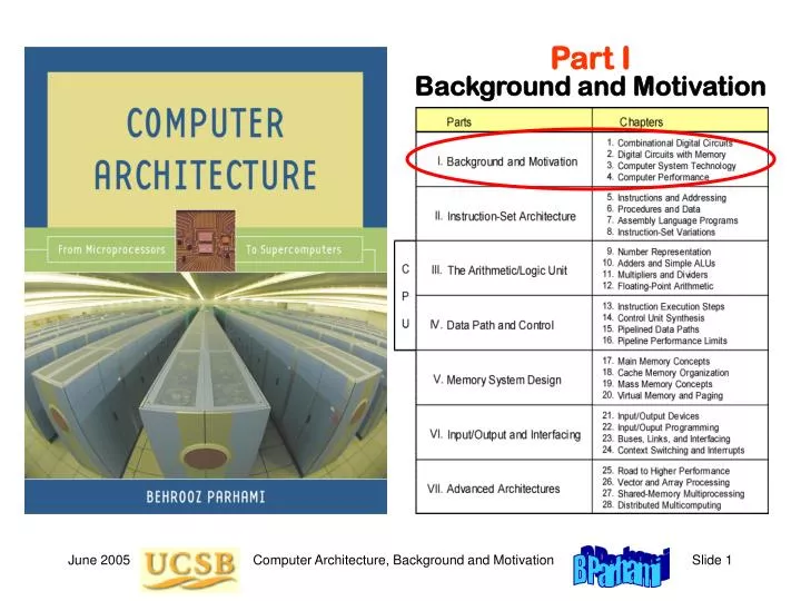
Part I Background and Motivation. I Background and Motivation. Provide motivation, paint the big picture, introduce tools: Review components used in building digital circuits Present an overview of computer technology Understand the meaning of computer performance

E N D
Part IBackground and Motivation Computer Architecture, Background and Motivation
I Background and Motivation • Provide motivation, paint the big picture, introduce tools: • Review components used in building digital circuits • Present an overview of computer technology • Understand the meaning of computer performance • (or why a 2 GHz processor isn’t 2 as fast as a 1 GHz model) Computer Architecture, Background and Motivation
1 Combinational Digital Circuits • First of two chapters containing a review of digital design: • Combinational, or memoryless, circuits in Chapter 1 • Sequential circuits, with memory, in Chapter 2 Computer Architecture, Background and Motivation
1.1 Signals, Logic Operators, and Gates Figure 1.1 Some basic elements of digital logic circuits, with operator signs used in this book highlighted. Computer Architecture, Background and Motivation
Variations in Gate Symbols Figure 1.2 Gates with more than two inputs and/or with inverted signals at input or output. Computer Architecture, Background and Motivation
Gates as Control Elements Figure 1.3 An AND gate and a tristate buffer act as controlled switches or valves. An inverting buffer is logically the same as a NOT gate. Computer Architecture, Background and Motivation
Wired OR and Bus Connections Figure 1.4 Wired OR allows tying together of several controlled signals. Computer Architecture, Background and Motivation
Control/Data Signals and Signal Bundles Figure 1.5 Arrays of logic gates represented by a single gate symbol. Computer Architecture, Background and Motivation
1.2 Boolean Functions and Expressions Ways of specifying a logic function Truth table: 2n row, “don’t-care” in input or output Logic expression: w (xyz), product-of-sums, sum-of-products, equivalent expressions Word statement: Alarm will sound if the door is opened while the security system is engaged, or when the smoke detector is triggered Logic circuit diagram: Synthesis vs analysis Computer Architecture, Background and Motivation
Manipulating Logic Expressions Table 1.2 Laws (basic identities) of Boolean algebra. Computer Architecture, Background and Motivation
Proving the Equivalence of Logic Expressions Example 1.1 Truth-table method: Exhaustive verification Arithmetic substitution xy = x + y-xy xy = x + y- 2xy Case analysis: two cases, x = 0 or x = 1 Logic expression manipulation Example: xy?xyxy x + y –2xy ?(1–x)y + x(1–y) –(1–x)yx(1–y) Computer Architecture, Background and Motivation
1.3 Designing Gate Networks AND-OR, NAND-NAND, OR-AND, NOR-NOR Logic optimization: cost, speed, power dissipation (xy) = xy Figure 1.6 A two-level AND-OR circuit and two equivalent circuits. Computer Architecture, Background and Motivation
BCD-to-Seven-Segment Decoder Example 1.2 Figure 1.8 The logic circuit that generates the enable signal for the lowermost segment (number 3) in a seven-segment display unit. Computer Architecture, Background and Motivation
1.4 Useful Combinational Parts High-level building blocks Much like prefab parts used in building a house Arithmetic components will be covered in Part III (adders, multipliers, ALUs) Here we cover three useful parts: multiplexers, decoders/demultiplexers, encoders Computer Architecture, Background and Motivation
Multiplexers Figure 1.9 Multiplexer (mux), or selector, allows one of several inputs to be selected and routed to output depending on the binary value of a set of selection or address signals provided to it. Computer Architecture, Background and Motivation
Decoders/Demultiplexers Figure 1.10 A decoder allows the selection of one of 2a options using an a-bit address as input. A demultiplexer (demux) is a decoder that only selects an output if its enable signal is asserted. Computer Architecture, Background and Motivation
Encoders Figure 1.11 A 2a-to-a encoder outputs an a-bit binary number equal to the index of the single 1 among its 2a inputs. Computer Architecture, Background and Motivation
1.5 Programmable Combinational Parts A programmable combinational part can do the job of many gates or gate networks Programmed by cutting existing connections (fuses) or establishing new connections (antifuses) Programmable ROM (PROM) Programmable array logic (PAL) Programmable logic array (PLA) Computer Architecture, Background and Motivation
PROMs Figure 1.12 Programmable connections and their use in a PROM. Computer Architecture, Background and Motivation
PALs and PLAs Figure 1.13 Programmable combinational logic: general structure and two classes known as PAL and PLA devices. Not shown is PROM with fixed AND array (a decoder) and programmable OR array. Computer Architecture, Background and Motivation
1.6 Timing and Circuit Considerations Changes in gate/circuit output, triggered by changes in its inputs, are not instantaneous Gate delay d: a fraction of, to a few, nanoseconds Wire delay, previously negligible, is now important (electronic signals travel about 15 cm per ns) Circuit simulation to verify function and timing Computer Architecture, Background and Motivation
Glitching Using the PAL in Fig. 1.13b to implement f = xyz Figure 1.14 Timing diagram for a circuit that exhibits glitching. Computer Architecture, Background and Motivation
CMOS Transmission Gates Figure 1.15 A CMOS transmission gate and its use in building a 2-to-1 mux. Computer Architecture, Background and Motivation