Download
1 / 25
280 likes | 582 Views
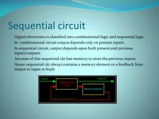
Sequential Circuit. Latch & Flip-flop. Contents. Introduction Memory Element Latch SR latch D latch Flip-flop SR flip-flop D flip-flop JK flip-flop T flip-flop. Introduction. Sequential circuit consists of feedback path and several memory elements

E N D
Sequential Circuit Latch & Flip-flop
Contents • Introduction • Memory Element • Latch • SR latch • D latch • Flip-flop • SR flip-flop • D flip-flop • JK flip-flop • T flip-flop
Introduction • Sequential circuit consists of feedback path and several memory elements • Sequential circuit = Combinational Logic + Memory Elements
Introduction • There are two types of sequential circuit • Synchronous – output change at certain time • Asynchronous – output change any time • Multivibrator – sequential circuit category – can be • Bistable – consist of two stable condition • Monostable – consist of one stable condition • Astable - no stable condition • Bistable logic device is latch and flip-flop • Latch and flip-flop differ by the method used to change stable condition
Memory Element • Memory element device that can remember a value for a certain period, or change value based on the input instruction • Example: Latch and flip-flop Commands for latches include set and reset commands
Memory Element • Flip-flop is a memory element which change its condition based on clock signal • Clock is a square waveform
Memory Element • There are two types of trigger/activator • Pulse triggered • Edge triggered • Pulse triggered • Latch • ON=1, OFF=0 • Edge triggered • Flip-flop • Positive edge triggered (ON=when 0 to 1, OFF=other time) • Negative edge triggered (ON=when 1 to 0, OFF=other time)
SR Latch • Output has complement: Q and Q’ • When Q HIGH, latch in SET condition • When Q LOW, latch in RESET condition • For SR with active high input (also known as NOR gate latch) • R = HIGH (and S=LOW) – RESET condition • S = HIGH (and R=LOW) – SET condition • Both LOW – no condition change • Both HIGH - Q and Q’ becomes LOW (invalid)
SR Latch with Gate • SR latch + enable (EN) input amd 2 NAND gate - SR Latch with Gate
SR Latch with Gate • Output change (if needed) only when EN at HIGH condition • Which condition is invalid? • Criteria Table
D Latch with Gate • Make input R the same as S’ - D Latch with Gate • D latch eliminate invalid condition in SR latch
D Latch with Gate • When EN is HIGH • D=HIGH – latch is in SET • D=LOW – latch is in RESET • Therefore, when EN is HIGH, Q will follow input D • Criteria Table:
Edge Triggered Flip-flop • Flip-flop – bistable synchronous device • Output change its condition at certain point on input trigger named clock • Condition change either at positive edge (up edge) or at negative edge (down edge) of clock signal clock signal Positive Edge Negative Edge
Edge Triggered Flip-flop • flip-flop SR, D and JK edge triggered is marked with “>” symbol at clock input Positive edge triggered flip-flop Negative edge triggered flip-flop
SR Flip-flop • SR flip-flop, at edge triggered clock pulse • S=HIGH (and R=LOW) – SET condition • R=HIGH (and S=LOW) – RESET condition • Both input LOW – no change • Both input HIGH - invalid • Criteria table of edge triggered SR flip-flop
SR Flip-flop • It consist of three parts • NAND latch • Pulse steering circuit • Pulse transaction circuit detector (or edge detector) • Pulse transaction detector circuit will detect up trigger (or down) and produce very short duration spike
D Flip-flop • D flip-flop: one input D (data) • D=HIGH – SET condition • D=LOW – RESET condition • Q will follow D at clock edge • To change SR flip-flop to D flip-flop: add inverter
D Flip-flop • Usage: Parallel data transaction To transfer logical output circuit X,Y,Z to Q1, Q2, and Q3 to be stored
JK Flip-flop • There is no invalid condition • There is toggle condition • J=HIGH (and K=LOW) – SET condition • K=HIGH (and J=LOW) – RESET condition • Both input LOW – no change • Both input HIGH – “toggle”
JK Flip-flop • JK Flip-flop • Criteria Table
T Flip-flop • T flip-flop single input version for JK flip-flop, formed by combining JK input • Criteria Table
T Flip-flop • Usage: As frequency divider
Asynchronous Input • SR input, D and JK is synchronous input. Where data from input will be transferred to flip-flop output only when edge triggered of clock pulse • Asynchronous Input free change condition from pulse clock. Example: preset (PRE) and clear (CLR) [or direct set (SD) and direct reset (RD)] • When PRE=HIGH, Q immediately HIGH • When CLR=HIGH, Q immediately LOW • Flip flop function as normal when both PRE and CLR is LOW
Asynchronous Input • JK flip-flop with active LOW preset and clear
Master Slave Flip-flop • Master is activated when positive edge and Slave is activated when clock negative edge triggered • Master Slave Flip-flop