Download

1 / 35
350 likes | 550 Views
Sequential Circuit Design. COE 202 Digital Logic Design Dr. Muhamed Mudawar King Fahd University of Petroleum and Minerals. Presentation Outline. The Design Procedure Moore Sequence Detector Mealy Sequence Detector Tracing State Diagrams and Verifying Correctness Sequential Comparator

E N D
Sequential Circuit Design COE 202 Digital Logic Design Dr. MuhamedMudawar King Fahd University of Petroleum and Minerals
Presentation Outline • The Design Procedure • Moore Sequence Detector • Mealy Sequence Detector • Tracing State Diagrams and Verifying Correctness • Sequential Comparator • Binary Counter • Up/Down Counter with Enable
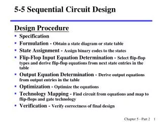
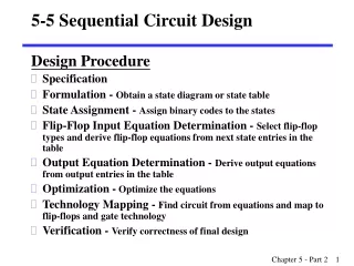
The Design Procedure Given a Description (or Specification) of the Problem • Obtain a state diagram for the sequential circuit • Assign binary codes to the states and fill the state table • Select the type of Flip-Flops and derive the FF input equations • Derive the output equations • Draw the circuit diagram • Verify the correctness of the final design (verification)
The State Diagram • A state is an abstraction of memory • A state remembers a history of inputs applied to the circuit • Examples: • State S0 represents the fact that the last input is a 0 • State S1 represents the fact that the last input is a 1 • State S2 represents the fact that the last two-input sequence is "11" • Obtaining the state diagram is the most important step • Requires experience and good understanding of the problem
Example: Sequence Detector • A sequence detector is a sequential circuit • Detects a specific sequence of bits in the input • The input is a serialbit stream: One input bit is fed to the sequence detector each cycle • The output is also a bit stream: One output bit each cycle Indicates whether a given sequence is detected or not Sequence Detector
State Diagram for a Sequence Detector • Example: Design a circuit that detects the input sequence "111" • Begin in an initial state: call it S0 S0 indicates that a 1 is NOT detected yet As long as the input is 0, remain in the initial state S0 • Add a state (call it S1) that detects the first 1 in the input • Add a state (call it S2) that detects the input sequence "11" • Add a state (call it S3) that detects the input sequence "111" 0 1 1 1 S0 S1 S2 S3
Complete the State Diagram Moore Design: Assign Output to States The output in S0, S1, and S2 should be 0 The output in S3 should be 1 0 0 S0 0 S1 0 S2 0 S3 1 1 Now complete the state diagram: Add transitions from S1, S2, S3 back to S0 if the input is 0 Add transition from S3 to itself if the input is 1 to detect sequences longer than three 1's 0 0 1 1 1
State Assignment • Each state must be assigned a unique binary code • If there are states then The minimum number of state bits: is the smallest integer ≥ (ceiling function) • In our example, there are four states: S0, S1, S2, and S3 Therefore, the minimum number of state bits (Flip-Flops) = 2 • State assignment: S0 = 00, S1 = 01, S2 = 10 and S3 = 11 • If bits are used, the number of unused states = • In our example, there are NO unused states
From State Diagram to State Table 0 0 S0 0 S1 0 S2 0 S3 1 1 0 0 1 1 State Assignment S0 = 00, S1 = 01 S2 = 10, S3 = 11 1
Structure of a Moore Sequence Detector • In our design examples, only D-type Flip-Flops will be used • They are the simplest to analyze and implement • Next, we need minimal expressions for • Next State Logic • Output Logic Next State Current State Next State Logic D Flip Flops Output Logic clock
Derive Next State an Output Equations 0 0 1 1 Two D-type Flips-Flops Present State = Flip-Flop Outputs and Next State = Flip-Flop Inputs and Next State equations: and Output equation: (from the state diagram) 0 0 0 0 0 0 0 0 1 1 0 1 1 1 0 1 00 00 01 01 11 11 10 10
Draw the Moore Sequence Detector Circuit , Next State Logic Output Logic
Mealy Type Sequence Detector • Let us redesign a Mealy type "111" sequence detector • The initial state S0indicates that a 1 is NOT detected yet As long as the input is 0, remain in the initial state S0 Notice that input / output is written on the arc (Mealy type) • Add a state (call it S1) that detects the first 1 in the input • Add a state (call it S2) that detects the input sequence "11" S1 S2 1 /0 1 /0 0 /0 S0
Complete the Mealy State Diagram • State S2 is reached after detecting the input sequence "11" • At S2, if the next input is 1 then the output should be 1 Make a transition from S2 back to itself labeled 1 / 1 No need for state S3, because output is on the arc • Now complete the state diagram Add transitions from S1 and S2 back to S0 when input is 0 S1 S2 1 /0 1 /0 0 /0 Mealy Machines typically use less statesthan Moore Machines 0 /0 1 /1 0 /0 S0
State Assignment and State Table Three States Minimum number of state bits (Flip-Flops) = 2 Assign: S0 = 00, S1 = 01, and S2 = 10 (State 11 isUnused) S1 S2 1 /0 1 /0 0 /0 0 /0 1 /1 0 /0 S0
Derive Next State and Output Equations 0 0 0 1 1 1 Present State = Flip-Flop Outputs and (state 11 is unused) Next State = Flip-Flop Inputs and Flip-Flop Input equations: and Output equation: 0 X X 0 0 0 X 0 0 0 0 0 1 0 1 0 X 1 0 X X 0 0 1 00 00 00 01 01 01 11 11 11 10 10 10
Draw the Mealy Sequence Detector Circuit Next State Logic Output Logic Next State Logic Reset
Mealy versus Moore Sequence Detector Mealy Sequence Detector Moore Sequence Detector In general, Moore state diagrams have more states than corresponding Mealy. The drawback of Mealy is that glitches can appear in the output if the input is not synchronized with the clock. 0 0 S1 S2 S3 1 S2 0 S0 0 S1 0 1 /0 1 /0 1 0 0 1 0 /0 0 /0 1 /1 1 0 /0 S0 1
Verification • Sequential circuits should be verified by showing that the circuit produces the original state diagram • Verification can be done manually, or with the help of a simulation program • All possible input combinations are applied at each state and the state variables and outputs are observed • A reset input is used to reset the circuit to its initial state • Apply a sequence of inputs to test all the state-input combinations, i.e., all transitions in the state diagram • Observe the output and the next state that appears after each clock edge in the timing diagram
Input Test Sequence • Required to verify the correct operation of a sequential circuit • It should test each state transition of the state diagram • Test sequences can be produced from the state diagram • Consider the Mealy sequence detector, starting at S0(reset), we can use an input test sequence to verify all state transitions: Input test sequence: reset then x = 0,1, 0, 1, 1, 0, 1, 1, 1, 1 S1 S2 1 /0 1 /0 reset 0 /0 0 /0 1 /1 Reset input forces initial state to be S0 0 /0 S0
Verifying the Mealy Sequence Detector Input test sequence: reset then x = 0,1, 0, 1, 1, 0, 1, 1, 1, 1 S2 S1 1 /0 1 /0 reset cc0 0 cc1 0 S0 1 cc2 0 S0 cc3 0 0 S1 0 S0 cc4 1 cc5 0 S1 1 0 cc6 S2 0 1 S0 cc7 0 S1 0 1 cc8 1 S2 1 cc9 cc10 S2 1 1 clock reset 0 /0 0 /0 1 /1 x Q1 0 /0 S0 Q0 glitch z
Sequential Comparator Problem Description: • Design a sequential circuit that compares two numbers A and B • Two Inputs: A and B A consists of n bits B consists of n bits Bit streaming starting at bit 0 Compare A0 with B0, A1 with B1, etc. (Bit 0 is least significant bit) • A reset signal resets the comparator to its initial state Reset is required before starting a new comparison • Two outputs: GT (Greater Than) and LT (Less Than) Sequential Comparator
Designing the State Diagram Moore State Diagram • Reset: start initially in state EQ EQ indicates Equality (output is 00) Stay in EQ as long as AiBi = 00 or 11 • Go to LT if Ai < Bi (AiBi = 01) LTindicates Less Than (output is 01) • Go to GTif Ai> Bi (AiBi = 10) GT is Greater Than (output is 10) • Complete the state diagram LT GT and GT LT LT LT and GT GT 00, 11 GT 10 LT 01 EQ 00 Reset 01 10 01 10 00, 11, 10 00, 11, 01
State Assignment and State Table Three States Two Flip-Flops D-type Flip-Flops will be used State Assignment: EQ= 00, LT= 01, GT= 10 Output = Present State (Q1 and Q0) 00, 11 GT 10 LT 01 EQ 00 Reset 01 10 01 10 00, 11, 10 00, 11, 01
Deriving the Next State Equations State 11 is unused When present state is 11, don't cares are used to fill the next state. Output = Present state 00 00 01 01 11 11 10 10 00 00 0 0 1 0 0 0 0 1 01 01 1 0 0 1 0 1 0 1 X X X X X X X X 11 11 0 1 0 1 0 1 0 1 10 10
Designing with Unused States • A circuit with n flip-flops has 2n binary states • However, the state diagram may have m states • Therefore, the number of unused states = 2n – m • Unused states do not appear in the state diagram • Sometimes treated as don't cares when simplifying expressions in K-maps • However, it is possible to enter an unused state! • Caused by outside interference or a circuit malfunction • Must specify the output and next state values for unused states • A special (invalid) output can be used to indicate an unused state • A return to a valid state must be possible without reset • Next state for unused states should be specified (NOT don't cares!)
Design of a Binary Counter Problem Specification: • Design a circuit that counts up from 0 to 7 then back to 0 000 001 010 011 100 101 110 111 000 When reaching 7, the counter goes back to 0 then goes up again • There is no input to the circuit • The counter is incremented each cycle • The output of the circuit is the present state (count value) • The circuit should be designed using D-type Flip-Flops
Designing the State Diagram • Eight states are needed to store the count values 0 to 7 • No input, state transition happens at the edge of each cycle S0 Three Flip-Flops are required for the eight states S7 S1 S6 S2 Each state is assigned a unique binary count value S5 S3 S4
State Table Only two columns: Present State and Next State State changes each cycle 000 111 001 110 010 101 011 100
Deriving the Next State Equations 0 0 1 1 ⨁ 0 1 1 1 1 1 1 0 1 0 1 0 0 1 0 0 0 0 00 00 0 0 00 01 01 0 1 01 11 11 1 0 11 10 10 1 1 10
3-Bit Counter Circuit Diagram ⨁ Output = 3-bit Count Value
Up/Down Counter with Enable Problem Specification: • Design a 2-bit Up / Down counter • Two inputs: E (Enable) and U (Up) If E = 0 then counter remains in the same state (regardless of U) If EU = 11 then count up from 0 to 3, then back to 0 If EU = 10 then count down from 3 down to 0, then back to 3 • The output of the counter is the present state (count value) • The circuit should be designed using T Flip-Flops • A reset signal resets the counter to its initial state
Designing the State Diagram • Four states are required to store the count 0 to 3 • Count up if EU = 11 • Count down if EU = 10 • Disable counter if E = 0 Transition to same state if EU = 00 or 01 • Asynchronous reset to start initially at state S0 E = 0 E = 0 EU = 10 S0 S1 Reset EU = 11 EU = 11 EU = 11 EU = 10 EU = 10 S3 S2 EU = 11 EU = 10 E = 0 E = 0
State Assignment and State Table • Four States Two State variables (2 Flip-Flops) • State Assignment: S0 = 00, S1 = 01, S2 = 10, and S3 = 11 E = 0 E = 0 EU = 10 00 01 Reset EU = 11 EU = 11 EU = 11 EU = 10 EU = 10 11 10 EU = 11 EU = 10 E = 0 E = 0