Download
1 / 30
300 likes | 437 Views
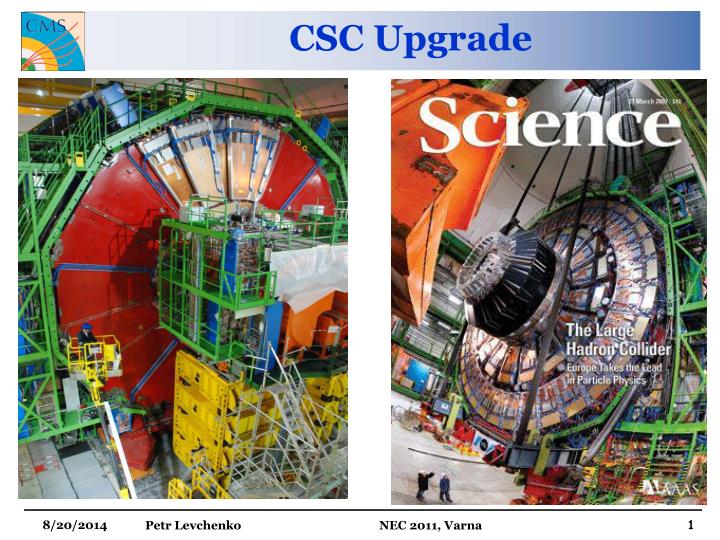
CSC Upgrade. CMS Endcap Region. CSC Upgrade. Scope Original design unfinished – ME4/2 not built 72(67) ME4/2 chambers to complete system Increase redundancy of system – 3 year run without access to do repairs Efficient triggering at high luminosities

E N D
CSC Upgrade Petr Levchenko NEC 2011, Varna
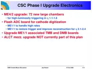
CSC Upgrade • Scope • Original design unfinished – ME4/2 not built • 72(67) ME4/2 chambers to complete system • Increase redundancy of system – 3 year run without access to do repairs • Efficient triggering at high luminosities • New digital CFEB boards for ME1/1 (part of M&O) • Increased capacity for data rate • Ungang the ME1/1 strips – 7 CFEBs per chamber instead of 5 • 72 New Datamother (DMB) boards • Replace of 72 ME1/1 Trigger Mother Boards (M&O) • Improve triggering for h = 2.1 to 2.4 Petr Levchenko NEC 2011, Varna
ME1/1 Upgrade Overview • ME1/1 Electronics replacement is designed to • Eliminate ME1/1a strip ganging • Provide deadtimeless readout (including at SLHC rates) • Improve triggering for |h|>2.1 • Liberate CFEBs for ME4/2 • Major components • New Digital Cathode Front End Boards (DCFEBs), 7/ME11 chamber • New Trigger Mother Board (TMB) Mezzanine card • New Optical Data Motherboard (ODMB) • Optical transmission of signals from DFEB to ODMB and TMB • New Low Voltage Distribution Boards (LVDB) and Low Voltage Mother Boards (LVMB) Petr Levchenko NEC 2011, Varna
Strips: 1 16 17 32 33 48 … … … Electronics Channel 1 … Channel 16 Strip Ganging in ME1/1a 48 strips of ME1/1a are ganged 3:1 into 16 readout channels: 1+17+33 strips into the 1st channel 2+18+34 strips into the 2nd channel etc This feature leads to triple ambiguity (ghost segments) and compromises trigger efficiency at high rates Solution:use of 3 CFEB boards instead of one for ME1/1a Petr Levchenko NEC 2011, Varna
Trigger Motherboard TMB Mezzanine prototype ● Need to implement more complex algorithms to increase trigger stub finding efficiency for high eta 2.1 < I η I < 2.4 with unganged ME1/1a ● Compatibility with seven new DCFEBs which provide comparator outputs for the CLCT processor New components of TMB Mezzanine => extra optical transceivers, EPROM are the platform for radiation tests of these components at the Texas A&M cyclotron (60 MeV protons) Petr Levchenko NEC 2011, Varna
DAQ Motherboard ● Replace 5 copper cables to CFEB with 7 optical links to DCFEB ● Developing radiation tolerant FF-EMU ASIC (IBM CMOS 130 nm) for the integrated distribution of TTC signals and for the data readout ● Implement all FIFO buffers inside the Virtex-6 FPGA ● Custom backplane connections remain unchanged Petr Levchenko NEC 2011, Varna
Present CFEB Petr Levchenko NEC 2011, Varna
Present Cathode Front-End Board ● 4..5 CFEBs per chamber ● 6 planes x 16 strips = 96 strips per CFEB ● 96 switch capacitors per channel, or 96 x 50 ns = 4.8 us Petr Levchenko NEC 2011, Varna
New DCFEB Petr Levchenko NEC 2011, Varna
DCFEB Prototype ● Same size as old CFEB board ● Same input connections and 6 BUCKEYE amplifier-shaper ASICs ● 12 Texas Instruments ADS5281 ADC (8-channel, 12-bit, 50 MSPS, serial LVDS output) ● 4 options for preamp/ADC interface to evaluate ● 2 legacy skewclear connectors compatible with old TMB and DMB ● 3.2Gbps optical links to new TMB and new DMB ● Xilinx XC6VLX130T-FFG1156 FPGA (~$1,200) ● 20-layer PCB Petr Levchenko NEC 2011, Varna
DCFEB R&D prototype • Two cards received in mid-March • Fab: Compunetics • assembly: Dynalab • Prototype tests at OSU: • many initial problems (odd/even pedestal differences, some FADC’s not working, PROM not working, bad voltage regulators, but all working now • analog part tested and input coupling scheme decided • One board currently at CERN for testing with real CSC chamber in Bat 904 • (see following slides from Stan Durkin) Petr Levchenko NEC 2011, Varna
DCFEB Prototype Channel Noise Stan Durkin DCFEB Pedestals – Typical Chip DCFEB and CFEB1 Noise RMS(ADC counts) ADC counts CFEB 1 DCFEB Channel Channel DCFEB Prototype Quieter than Old CFEB No SCA so noise reduces by 1.3 ADC counts in quadrature Petr Levchenko NEC 2011, Varna
LVDB and LVMB boards • New Low Voltage Distribution Boards for ME1/1 • Changes • 7 DCFEBs • additional temperature sensors • additional DAC reference voltage • new connector types • Latch-up protection diodes • JINR/NCpHEP responsibility • Prototypes set up for production • Test setup in ISR • New Low Voltage Mother Board • New interface to ODMB • Support for additional voltage controls • Under study by UC Davis (Britt Holbrook) Old LVDB Section of layout of new LVDB prototype Petr Levchenko NEC 2011, Varna
Physical Installation Mockup Mockup of the new LVDB and DCFEBs on ME1/1CSC Vladimir Karjavine
Scope of ME4/2 Project • Chambers • Build 72 chambers to complete the 4th station • Build & operate a new factory in B904 • Use some on-chamber electronics from ME1/1 • Construct/build infrastructure (electronics, power, cooling, etc.) to operate these chambers Petr Levchenko NEC 2011, Varna
10m Chamber storage area 6m 5m 25m 10m Strip gluing Gas Packing 7m Long term gas & HV Electronics assembly Fast site testing Panel cleaning/gluing Loading area 20m 6m Kit preparation platform clean Lab 2 clean Lab 1 hand soldering Incoming parts 7m panel storage 10m 10m 15m 15m Chamberrack Chamber production workflow • Incoming parts • Kit preparation • Panel bar gluing • Wire wiring, gluing, soldering (Lab 1) • Electrical components hand soldering • Chamber assembly & test (Lab 2) • Long term gas, HV tests • Electronics assembly & Fast site test • Final inspection packing, storing Petr Levchenko NEC 2011, Varna
Panel gluing Anode wire fixation bars Glue dispenser Cathode gap bars Petr Levchenko NEC 2011, Varna
Clean room 1: Winding • About 1000 50μm thick AuW wires are winded on the anode panel with a ~3.16mm pitch. Total wire length ~2600 m per panel. Winding time: ~4h per panel. 200 μm thick field-shaping CuBe wires are tensioned (500g) and soldered beforehand • Then, mylar fixation strips are glued onto the wire-end before wire soldering Petr Levchenko NEC 2011, Varna
Clean room 1: Automatic wire soldering • Automatic wire soldering is done using the Panasonic machine. Re-commissioning of the machine was successfully done (O. Prokofiev FNAL) Petr Levchenko NEC 2011, Varna
Component soldering area Hand soldering of components (R, C), connectors, ground strip on panels • 2 fully equipped soldering stations with local smoke extractors Petr Levchenko NEC 2011, Varna
Completed anode panel Petr Levchenko NEC 2011, Varna
Clean room 2: Panel assembly Ionized air gun gas HV rack TMB Mezzanine Assembly tables • 4 Cathode and 3 anode panels are cleaned, tested, assembled and sealed using two assembly tables (surveyed to better than 1mm flatness) • Chamber is tested for leaks and HV (1 day) Petr Levchenko NEC 2011, Varna
Chamber assembly • Assembly operations: • cathode panels continuity check • anode panels electrical tests (wire capacitance, HV, • prepare for chamber assembly • clean panels using ionized air knife • position chamber frames and dry assembly • continue electrical tests • chamber RTV sealing • install HV cables and ground foil • assembly chamber frames • short term HV training and leak test (with Ar) • Benchmark ~28h chamber for assembly + ~1day for testing. FNAL factory ! Petr Levchenko NEC 2011, Varna
Long term test area • Assembled chambers will be placed on a 8 chamber rack to undergo long term (~2 months) HV training (3.6-3.8 KV) and leak test • Standard ArCO2CF4 gas mixture is used. Anticipated gas costs are ~12 KCHF/year PSL design Petr Levchenko NEC 2011, Varna
Electronics integration & chamber testing • On-chamber electronics integration and full (fast-site) testing will be part of the production workflow: • mount/test cooling plate • strip/wire r/o electronics and cables • LV distribution & monitoring boards • For chamber testing we will use upgraded test stand with the new h/w and s/w AFEB Test Stand has been revised: ● Measure basic characteristics of AFEB amplifier-discriminator chip (CMP16) and board (AD16) ● Tabletop setup ● Developed at Carnegie Mellon University ~10 years ago ME4/2 Project Progress Review (AL UW)
Factory labor Present FTEs • 1 FTE from UW (Factory Manager) • 1 FTE from CERN (Floor Manager) • 3 FTE from PNPI (Production Eng. + 2 production Eng/Tech) • Should become 4 FTE from September (+1 prod. Tech) • 2 FTE from IHEP (Production Tech + Student/Supervisor) • 1 FTE from UCSB (Production Tech) • ~2 FTE from UCLA+PNPI (Physicists, Prod. Eng, Prod. Tech) Tot: ~11 FTE Expected FTEs: Tot: ~ 13 FTE Caveat: Some of the people are key experts within CMS TC and will be required to intervene during extended technical stops for detector and infrastructure maintenance [S. Kreyer (tracker cooling), S. Di Vincenzo (beam pipe, infra), AL(CSC)] Petr Levchenko NEC 2011, Varna
people The golden team Petr Levchenko NEC 2011, Varna
Summary • CSC Upgrade will be essential as luminosity increases. • ME1/1 electronics design, prototyping etc.. In progress. • ME4/2 Factory site available & operational in 2011. • Delays will make it difficult to install CSC according to CMS plans Petr Levchenko NEC 2011, Varna