Download
1 / 46
470 likes | 485 Views
Electron Microscopy - References. Buseck, Cowley and Eyring, “High-Resolution Transmission Electron Microscopy” (Oxford Univ. Press, 1988). Cowley, “Diffraction Physics”, (North-Holland, 1975). Edington, “Practical Electron Microscopy in Materials Science” (van Nostrand, 1976).

E N D
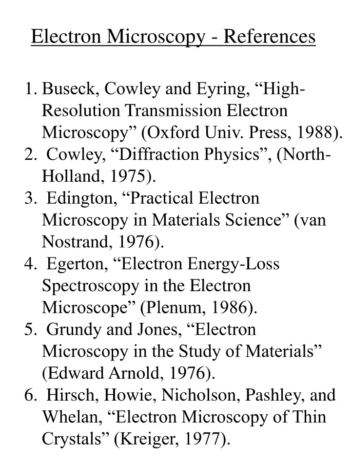
Electron Microscopy - References • Buseck, Cowley and Eyring, “High-Resolution Transmission Electron Microscopy” (Oxford Univ. Press, 1988). • Cowley, “Diffraction Physics”, (North-Holland, 1975). • Edington, “Practical Electron Microscopy in Materials Science” (van Nostrand, 1976). • Egerton, “Electron Energy-Loss Spectroscopy in the Electron Microscope” (Plenum, 1986). • Grundy and Jones, “Electron Microscopy in the Study of Materials” (Edward Arnold, 1976). • Hirsch, Howie, Nicholson, Pashley, and Whelan, “Electron Microscopy of Thin Crystals” (Kreiger, 1977).
Electron Microscopy - References 7. Hren, Goldstein and Joy, “Introduction to Analytical Electron Microscopy” (Plenum, 1979). 8. Joy, Romig and Goldstein, “Principles of Analytical Electron Microscopy” (Plenum, 1986). 9. Loretto, “Electron Beam Analysis of Materials” (Chapman and Hall, 1984). 10. Reimer, “Transmission Electron Microscopy” (Springer Verlag, 1985). 11. Thomas and Goringe, “Transmission Electron Microscopy of Materials” (Wiley, 1979). 12. Williams, “Practical Analytical Electron Microscopy in Materials Science” (Philips, 1984).
Electron Microscopy Electron-Matter Interactions Inelastic Scattering Elastic Scattering Electron Diffraction Electron Imaging Chemical Analysis Structure Microscopy
Electron Microscopy Microscopy Magnification Contrast Spatial Resolution
Electron Imaging Systems • Unlike x-rays, electrons may be focused to form an image diffraction pattern (Fourier transform) image object so f f si
Diffraction in Imaging Systems • Slits, lenses, etc. in imaging systems act as • apertures resulting in diffraction • Image points are diffraction patterns not points Image point with diffraction Imaging System I O Object Image Imaging system with circular aperture (e.g., telescope, light microscope, electron microscope)
Fraunhofer (Far-Field) Diffraction Pattern from a Circular Aperture Airy disk I(q)/I(0) Dq g • J1(g) = 0 when g = ½kDsinq ≈ 3.832 • sinq≈ 1.22l/D • Dq ≈ 2 (1.22l/D)
Spatial Resolution • Spatial Resolution = the minimum separation between two points in the object that can still be observed as separate in the image • If aberrations are corrected then we say the optics • are diffraction-limited overlapping diffraction patterns Imaging System Object Image From Pedrotti & Pedrotti, Fig. 16-8, p. 336
Rayleigh’s Criteria I(q)/I(0) Dq= 1.22l/D “just” resolvable q I(q)/I(0) Dq< 1.22l/D not resolvable q
Spatial Resolution Dqmin= 1.22 l/D xmin = f Dqmin = 1.22l (f/D) = 1.22l / 2NA NA = numerical aperture of lens Dqmin objective lens diameter, D xmin f
Microscope Resolution xmin = 0.61 l / NA • Improve resolution by reducing wavelength • Optical: l ~ 500 nm • xmin ~ 250 nm • Electrons: l = h / p • = h / (2moE)½ • = 1.22 / V (nm) • (non-relativistic, E << Eo = 511 keV) • E = 100 keV (typical) • l ~ 0.04 Å xmin ~ 0.02 Å (5 – 20 Å achieved in practice)
Conventional TEM (CTEM) Diffraction pattern formed in back focal plane From Williams, Fig. 1.3, p. 3
Image Formation diffraction orders diffraction pattern (Fourier transform) so f f si
Magnification(Optical Analogy) intermediate image Fo Fi Fi Fo virtual image (magnified) back focal plane
EM Lenses • Electron lenses are Cu windings that form a solenoid • Force on electron is • F = q (v x B) • Can focus/magnify image by adjusting lens currents (B) • Magnification up to 106 • Can image specimen or diffraction pattern by adjusting lens currents
Electron Microscope Specimen Image (microscopy) Crystal structure From Ohring, Fig. 6-10, p. 270
Electron Microscope • Microscope is under vacuum • (< 10-4 Torr) • Eliminate scattering of electrons from gas (need mean free path > 1 m) • Minimize contamination of specimen and microscope components
Electron Microscope Sources Filament current - 100 kV – 1 MeV + Electron beam
Electron Microscope Sources • Thermionic emission: thermal energy allows electrons to overcome work function of material (e.g., W or LaB6) • Field emission: electron can tunnel through surface potential barrier (e.g., W or ZrO-coated W) From Reimer, Fig. 4.1, p. 80
Microscope Resolution • In practice, resolution is limited by: • Dispersion (energy spread) and stability of electron source • Microscope aberrations • Energy loss & scattering of electrons in sample • Typical Resolution • ~ 5 - 10 nm (thermionic • emission) • ~ 0.5 – 2 nm (field emission)
Electron Detectors • Phosphor coated screen CRT) • Special photographic emulsions From Williams, Fig. 1.3, p. 3
Image Contrast • Amplitude and phase change of electron waves gives contrast Image Contrast Absorption Contrast Phase Contrast Diffraction Contrast
Image Contrast Contrast is formed by using aperture in back focal plane to block scattered electrons From Williams, Fig. 1.3, p. 3
Absorption Contrast • Increase in scattering (elastic and inelastic) with higher atomic number Z and thickness of material • Scattered electrons are blocked by objective aperture in rear focal plane producing darker contrast 10 nm carbon lead 9 96 17 91 83 4 objective aperture
Diffraction Contrast • Smaller lattice constant diffracts to larger angles • diffracted electrons blocked by aperture • darker contrast blocked electrons
Diffraction Contrast • Only one beam (transmitted or diffracted) is allowed to pass through the objective aperture • Incident beam → bright field • Diffracted beam → dark field z z transmitted beam diffracted beam transmitted beam 2q 2q diffracted beam Ewald sphere g Ewald sphere g aperture aperture Bright field Dark field
Phase Contrast The more diffraction orders captured, the greater the specimen detail that can be resolved (more Fourier components)
Fourier Analysis of Square Wave 0.5 0.5 + (2/p)sinkx 0.5 + (2/p)sinkx - (2/3p)sin3kx 0.5 + (2/p)sinkx - (2/3p)sin3kx + (2/5p)sin5kx
Phase Contrast • Can combine transmitted and diffracted beams to produce high-resolution lattice images • Uses amplitude & phase from Ohring, Fig. 14-17, p. 664
Electron Microscopy Electron Microscopy TEM (thin foil) SEM (bulk) small scanning electron beam (~ 50 Å) CTEM STEM large diameter (10’s mm’s) stationary electron beam small diameter (~ 10 Å) scanning electron beam
Conventional TEM (CTEM) • Large diameter, stationary electron beam (~10’s mm) From Williams, Fig. 1.3, p. 3
Scanning TEM (STEM) • Small diameter electron beam (~0.5 nm) scanned across surface From Williams, Fig. 1.7, p. 5
Scanning TEM (STEM) • An electron beam (incident into the page, along the z direction) will be deflected by a perpendicular magnetic field • The electron beam can be scanned in a raster pattern across the sample By Bx
Disadvantage of TEM : Sample Preparation • Specimen must be thin enough to transmit electrons • e.g., range of 100 keV electrons in Si ~ 0.6 mm • Sample preparation • Many hours • Epoxy sections together • Polish to produce thin foil • Ion beam milling (thin by sputtering) • Hole appears in middle • Thickness at edge of hole ~ 2000 Å
SEM • Incident electron energy ~ 1- 50 keV • Pairs of scanning coils (x, y) deflect a small diameter (~ 50 Å) electron beam across a specimen surface From Williams, Fig. 1.4, p. 3
SEM • Electrons undergo elastic and inelastic scattering with sample resulting in tear-shaped interaction volume • Inelastic processes include production of x-rays, secondary electrons, light, phonons, e-h pairs, Auger electrons Electron Beam Secondary electrons (1-10 nm) Auger electrons (1 nm) Backscattered electrons (0.1 – 1 mm) X-rays (0.2 – 2 mm)
SEM • Usually use secondary electrons (1 – 50 eV) to form SEM image • Secondary electrons: electrons in CB are ejected due to collision with incident electron (inelastic scattering) Elastic Backscattered Electrons Secondary Electrons Electron Yield Auger Electrons 5 2000 50 Eo Electron Energy (eV)
SEM • Secondary electrons • Originate from a depth < 10 nm • Surface-sensitive technique • Best resolution Probability of SE escape 1 0.5 50 75 0 25 Depth at which SE are generated (Å)
SEM • Low energy electrons are detected by scintillator (e.g., NaI) - PMT system From Williams, Fig. 1.14, p. 8
SEM • Edges and slopes appear brighter due to greater SE yield from volume projection Electron beam to SE detector
SEM • Can also use backscattered electrons • Backscattering yield is sensitive to the atomic number • Greater elemental sensitivity than secondary electrons
SEM • Image magnification : • M = scan length on CRT, L • scan length on specimen, l • Magnification achieved electronically by changing the scan area on the specimen via the scanning coils xxxx xxxxxx xxxx xxxxxx l L Area scanned on specimen Area scanned on CRT
SEM • Maximum magnification : • M = pixel size on CRT • beam diameter • ~ 105 xxxx xxxxxx xxxx xxxxxx l L Area scanned on specimen Area scanned on CRT
SEM • Can detect other signals in the SEM for compositional analysis • Cathodoluminescence (CL) • X-rays (EDX) • e-h pairs (EBIC) From Schroder, Fig. 10.4, p. 655
Channeling • Electrons incident along a major crystallographic orientation experience channeling effect • Electron backscattering yield is reduced
Channeling • Channeling pattern can be used to deduce crystal structure From Loretto, Fig. 4.20, p. 137