Download
1 / 23
230 likes | 386 Views
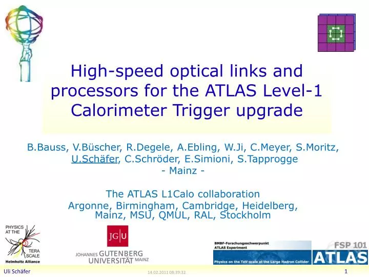
High-speed optical links and processors for the ATLAS Level-1 Calorimeter Trigger upgrade. B.Bauss , V.Büscher , R.Degele , A.Ebling , W.Ji , C.Meyer , S.Moritz , U.Schäfer , C.Schröder , E.Simioni , S.Tapprogge - Mainz - The ATLAS L1Calo collaboration

E N D
High-speed optical links and processors for the ATLAS Level-1 Calorimeter Trigger upgrade B.Bauss, V.Büscher, R.Degele, A.Ebling, W.Ji, C.Meyer, S.Moritz, U.Schäfer, C.Schröder, E.Simioni, S.Tapprogge - Mainz - The ATLAS L1Calo collaboration Argonne, Birmingham, Cambridge, Heidelberg, Mainz, MSU, QMUL, RAL, Stockholm 14.02.2011 08:39:32
Outline • Current Level-1 Calorimeter Trigger • Latency… • Upgrade for higher luminosity: Phase 1 • Towards Phase 2 • Mainz R&D activities
ATLAS Trigger / current L1Calo L1 Jet/Energy module µ calo CTP
Current L1Calo • Analog signal chain on- and off-detector • Mixed-signalPre-Processor with discrete analog and ASIC-based digital circuitry : digital filtering / gain control / bunch crossing ID • Digital processing: • Sliding windows algorithms for jet and em cluster detection on processor modules atgranularity ≥ .1×.1 (η×φ) • Data consolidation by thresholding and counting objects • Data transmission on parallel backplane to mergers (CMMs) • Global results determined by summation trees on daisy-chained merger modules • Final results of electromagnetic and hadronic object count (at given thresholds), and total and missing transverse energy reported to Central Trigger Processor • Topological information (Regions of Interest – ROIs – basically energy sumsper window) sent to 2nd level triggeronly for all level-1 accepted events slidingwindow
Latency, algorithms, data paths … Total latency limited to c. 2.5 microseconds (cables!) Sliding windows algorithms require duplication of data across processor module and crate boundaries All real-time data transmitted electrically • Analogue off the detector • 480 Mb/s differential into digital processors, data replication at source • 80 / 160 Mb/s single ended data replicated over a custom backplane • 40 Mb/s to, between & from merger modules (CMMs) System works well, latency limits met. Complicated and expensive processor backplane (18 layers) and considerable cable plant
The horror lurks behind… Jet/En. processor Jet/Energyprocessor Pre-processor
Upgrade : Re-think connectivity • Upgrade will require additional connectivity • System density will rule out additional electrical cabling • Latency might get even more critical • Go for optical connections • Increase system density by use of FPGA-internal Multi-Gigabit Transceivers (MGTs) • Accept inherently higher latency per high speed link • Partition the system such that excessive de-serialization/re-serialization is avoided • Optimize the data replication scheme • Explore options for latency reduction on the FPGA
Data replication Forward data replication only: • Duplication at source • Mirror a link • Assemble a different stream optimised for thereplication • Optical splitter (fibre coupler) Do not share any data between modules of same subsystem to avoid additional SerDes latency source sink
L1Calo upgrade steps Due to expected increase in pile-up of events at rising luminosities, the current algorithms will be degraded. Improve L1Calo in distinct phases • Phase 0 : • Some improvements on the FPGA based algorithms have been made and will be in use for 2011 running • Further optimizations might follow • No hardware being added / replaced at this stage • Phase 1 : • Improve digital signal processing on Pre-Processor ( ASIC FPGA ) • Add topological processing with limited hardware changes • Phase-2 : • Improve of granularity of L1Calo algorithms in η, φ, and depth • Replace Level-1 Calorimeter Trigger • Probably distinguish Level-0 and Level-1 trigger NB : • This is a snapshot of current thinking only. Level-1 technical proposal being written • Stages are related to, but not strictly dependent on the LHC machine upgrade steps • L1Calo will attempt to stage the installation of new hardware (sub-phases) • Phase-1 is mainly internal to L1Calo, no strict need for mods of external interfaces • Phase-2 is dependent on calorimeter readout electronics upgrade
Phase 1: Topology • So far topology of identified objects not propagated through 1st level trigger real-time data path for bandwidth reason • Increase RTDP bandwidth and send (almost) full ROI information to a single processor stage where topology cuts are applied and double counting is suppressed by jet/electron/... matching: • Increase backplane bandwidth of existent processor modules 4-fold (40Mb/s160Mb/s) with modification to FPGA code only • Replace the CMM merger modules by “CMM++” modules • Single FPGA processor • 64Gb/s backplane input capability • Possibly up to ~400Gb/s optical I/O • Star-couple all CMM++s into topological processor • Include Muon processing capability on topological processor • Backward compatible to current scheme(for staged installation) :CMM++ daisy-chain (electrical / optical)
New merger module: CMM++ VME -- VME CPLD Legacy DAQ, ROI readout (Glink) SNAP12 Topologicalprocessor links: 12-fiber bundles, 6.4/10 Gbit/s/fiber Virtex 6 HX565T LVDS merger links SNAP12 SNAP12 SNAP12 Backplane data from JEM/CPM modules (160 MHz) Legacy LVDS outputs to CTP SNAP12 SNAP12 9U × 40 cm
L1Calo Phase-1 • Daisy chained • Combination of low-latency LVDS + high bandwidth opto links CMM++ Full system w.topo processor single crate
eventually … Phase 2 ! « Once the calorimeter readout is replaced … in 20xx … » • High granularity trigger data provided on optical links • New sliding windows processor with optical interfaces only • Synchronous low-latency L0 plus asynchronous L1
Upgrade activities in Mainz • Simulations of topological algorithms at high luminosities (1034 cm-2s-1), high pile-up • Simulation and implementation of the algorithms in VHDL • Improvements on VHDL code for current processors • Design of demonstrator modules for phase 1 and phase 2 • Topological processor • Phase-2 Level-0 sliding windows processor • Latency optimization • Data replication schemes • FPGA on-chip MGT operation modes and fabric interfaces
Demonstrators / Prototypes so far… • Work on a CMM++ prototype has started recently at MSU. Currently at specifications stage. Will serve as data input for the topological processor • “GOLD” demonstrator (not just) for a topological processor currently being developed in Mainz Latency data replication schemesDensity processing power, connectivity • Mainz-built “BLT” backplane and link tester, equipped with Avago opto-link interface (12-channel, 6.4Gb/s) and LHC bunch clock jitter cleaning hardware.Successfully verified backplane data reception (160Mb/s) and opto link operation.
GOLD – Generic Opto Link Demonstrator «data concentrator» scheme:many in – few out • Advanced TCA form factor • Limited connectivity on front panel • Input links via optical connectors in zone 3 • 12-channel 10Gb/s opto modules on daughter card • Electrical connectivity up to 10Gb/s in zone 2 • Power budget ~400W • RTM • front • Z3 • back • Z2 • ATCA
GOLD • Z3 • 5 * XC6VLX FPGAs(Input L, main M) up to 36 links each • Two pairs of XC6VHX FPGAs (H) 72 links • Up to 12 12-channel optos on mezzanine • Clock generation • 144 multigigabit links in zone 2 (equiv. 22300 bit / BC) • L • L • Opto • M • L • L • H • H • Z2 • 890Gb/s • total • H • H • Z1
Module status • Main board finished • Carefully hand-routed (~ 400 differential pairs per FPGA, line rates 1.0/6.5/10 Gbps) • Daughter modules almost done • Will have several incarnations of daughter modules • L1Calo-internal review soon • Components available …
Components… opto mezzanine datareplicationatCML level 12 to 72 fibres per backplane connector (MPO/MTP) 10Gb/s Opto clockmezzanine
Current activities: h/w, f/w • Main focus on GOLD hardware design / production • First module tests spring 2011, further hardware development for phase1 Topo-processor and phase2 (Virtex-7, up to 28Gb/s) • Characterize 6.5/10Gbps optical link chipsets (Avago) • Work on latency minimization for Xilinx MGTs operated synchronous to LHC bunch clock, with phase alignment GTX receiver Receivedclock | LHC clock
Some current activities • Default encoding (for phase 1 topo) 8b/10b, 80% payload • Successfully tested a variant for latency critical paths: • Transmit raw data, alternating normal and inverted representation • 50% payload, latency reduction by c. 1 LHC bunch tick • Suppression of elastic buffer • Works out of the box with Xilinx IP core for small channel count • Fails for large channel count due to insufficient global routing resources • Will probably require to devise specific scheme for re-synchronisation to global LHC bunch clock
Summary / outlook • Need for substantial improvement of trigger algorithms • Topological processor (phase-1) and new sliding windows processor (phase 2) require high-density processors with high-speed, low latency optical interconnect • For phase 1 explore 6.5/10 Gbps opto-links • For phase 2 explore 10/13/28 Gb/s technology • Work on conceptualdesignsanddemonstratorsfor upgrade phases 1 and 2 hasstarted • Mainz active on hardware / firmware / simulation for both upgrade phases, with particular interest in low latency optical data transmission • Commission GOLD demonstrator in 2011 • Use as a starting point for phase-1 and phase-2 prototype development • Benefitfromsimilarrequirements on phase 1 and 2