Download
1 / 46
460 likes | 466 Views
This study focuses on accurately modeling and simulating conducted and radiated EMI from HPM and UWB sources on PCBs and ICs. It tackles the complexity of the system and develops methodologies for modeling the coupling path and EMI sources. The goal is to integrate these models into non-linear circuit simulators for efficient analysis.

E N D
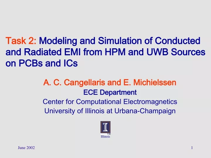
Task 2:Modeling and Simulation of Conducted and Radiated EMI from HPM and UWB Sources on PCBs and ICs A. C. Cangellaris and E. Michielssen ECE Department Center for Computational Electromagnetics University of Illinois at Urbana-Champaign
EMI to connectors & packages Antennas Cracks Apertures Cables Circuits Internal Coupling Propagation to interior HPM/UWB Sources Internal fields as radiated EMI Spurious behavior Objective • Accurately “propagate” the spurious signals (noise) through the packaging hierarchy (printed circuit boards, cards, connectors, interposer, package…) to the die.
Courtesy of Qualcomm Major Obstacle: Tackling System Complexity
System Complexity translates to EM Complexity • EM Complexity • Geometric complexity and distributed nature of the packaging hierarchy (“coupling path”) • Broad frequency bandwidth of the interfering signal • Non-linearity of the terminations • Tackling Complexity • Hierarchical approach to the modeling of electromagnetic interactions • From lumped models, to transmission-line models, to quasi-3D full-wave models, to 3D full-wave models • Abstracting Complexity • Systematic order reduction of numerical models of the coupling path • Equivalent circuit representation of the coupling path for its seamless incorporation in network-oriented non-linear circuit simulators
SUMMARY OF MODELING OBJECTIVE Radiated EMI Virtual coupling ports Integrating Substrate (PCB, MCM, …) Conducted & radiated EMI Packaged digital & analog devices Physical coupling ports (e.g., connectors, cables…) EM Modeling & Simulation Model Order Reduction Synthesis Equivalent source representation of radiated EMI coupling Source representation of conducted noise at the physical ports Network representation of the coupling path V Non-linear lumped circuits V
Specific Subtasks • Task 2.1Development of a coupling path modeling methodology • Task 2.2 Development of a (EMI) source modeling methodology • Task 2.3Non-linear Transient Simulation of the hybrid lumped-distributed non-linear network
IBM Corporation Printed Circuit Board Chip Package Subtask 1: Modeling of the Coupling Path
Subtask 1: Modeling of the Coupling Path (Cont) • Our modeling approach is hierarchical • EM-Physics driven “divide and conquer” approach • Use suitable EM modeling approach for individual blocks • RLC models for short interconnect at chip & package level • Multi-conductor Transmission Lines (MTL) • Balanced interconnects at the board level • Quasi-3D EM Modeling for PCB power delivery network • Full-wave modeling • Unbalanced interconnects at the board level • Coupling through cables • RF/microwave packages & boards • Reduction of EM models to non-linear network simulator (e.g. SPICE) • Direct model order reduction • Equivalent circuit synthesis
Quasi-3D Modeling of Power Delivery Network • EM field between power/ground plane • pairs exhibits, approximately, a two- • dimensional variation • Use simple 2D FDTD • Three-dimensional features (vias, pins, • slots, voids, etc) require locally 3D • models to capture the correct physics
The resulting discrete EM model • Direct time-domain simulation is possible if desired • Could be synchronized with time-domain IE solver • Alternatively, model order reduction of the transfer function • using an Arnoldi-based subspace iteration method (PRIMA) • is used for the generation of a compact multiport
Multi-port representation of the reduced-order model is in terms of rational functions • Form compatible with circuit simulators that support rational function models (e.g. H-Spice, ADS) • Equivalent circuit synthesis is possible also
The advantages of the direct use of the rational function macro-model in the simulator Elapsed Simulation Time Transient Data File Size The secret is in the recursive convolution that is utilized for the interfacing of the macro-model with the rest of the circuit
Application to a 4-layer PCB 8 cm X 4 cm, 4 layer board. A 2mm gap is present all the way across the top ground plane. A total of 58 pins are used. Top view |Z21| From H-SPICE Cross-sectional view
Application to a 4-layer PCB (cont’d) H-SPICE calculation of the transient response. Switching occurs at port 1 while port 2 is terminated with 50ohm. Voltage at port 1 is depicted by the solid line. Voltage at port 2 is depicted by the dotted line.
Validation study in progress Intel 4-layer test board 1st layer: Power plane 2nd layer: Ground plane 3rd layer: Ground plane 4th layer: Power plane
Generated multi-port for switching noise simulation in SPICE
Rational function multi-port & equivalent circuit synthesis from raw data • Data either from measurements or EM field solvers • Step 1: Rational function fitting • Process guarantees stability but not passivity • Check fitted multi-port for passivity • If not passive, constrain fitting using Foster constraints • Repeat fitting
Validation of rational function fitting PCB interconnect test structures courtesy of Intel
Validation of fitting (cont’d) Measured |Y61|* Synthesized |Y61| (*) Measurements courtesy of Intel Corporation
Task 2.1 Summary • EM modeling flow for the coupling path established • Quasi-3D EM Model for power delivery network completed • Validation in progress • Further enhancements include: • Incorporation of hooks for balanced MTLs • Incorporation of hooks for matrix transfer functions in Foster form • Capability for SPICE-compatible broadband multi-port macro-model generation in place
15 cm 20 cm 10 cm 15 cm 1 cm 1 cm 4.5 cm 17.5 cm 25 cm 25 cm 30 cm 30 cm Subtask 2.3:Non-linear Transient Simulation • Physics-oriented nonlinear transient simulator • Full wave modeling of printed circuit boards (PCBs) with fine geometric features, finite (and possibly inhomogeneous) dielectrics, and nonlinear loads and circuits • Interfaces with SPICE solvers and models
20 cm 10 cm 5 cm 1 cm 17.5 cm 0.5 cm 6 cm 4.5 cm 25 cm 25 cm varistor Introduction (cont.) • Time Domain Integral Equation (TDIE) based Marching-on-in-time (MOT) solvers • Have been known to the acoustics and electromagnetics communities since the sixties. • Compared to frequency domain solvers, they can solve nonlinear problems directly. Liu and Tesche (1976), Landt and Miller (1983), Djordjevic and Sarkar (1985), Deiseroth and Singer (1995), Orlandi (1996)
Introduction (cont.) However TDIE - MOT solvers have long been conceived as • Unstable:… But recently many proposals have surfaced for stabilizing these schemes (Davies, Rao and Sarkar, Walker, Smith, Rynne,…); • Slow:… Computational complexity has prohibited application to analysis of large scale problems!… PWTDtechnology removes this computational bottleneck Now, we can / should be able to rapidly solvelarge -scale, nonlinearproblems using the PWTD technology!!!
Formulation - Problem Definition • Given • an of 3-D inhomogeneous dielectric bodies (V ), and 3-D arbitrarily shaped PEC surfaces, wires, and surface-wire junctions (S), • Multiple linear / nonlinear lumped circuits connected to • a temporally bandlimited excitation ckt 1 interconnect geometry ckt m • Solve for • all transient currents and voltagesinduced on the interconnect geometry and the the circuits (ckt 1, …, ckt m) • radiated electric and/or magneticfields if required distributed lumped
Formulation –Time Domain Electric Field • Assume spatially-variable, frequency independent permittivity and free-space permeability in V, and thin wires in S . PEC • Radiated electric field: (1) (2)
Formulation - MOT Algorithm • Expand current as • Surface and Volume Spatial Basis Functions • The temporal basis functions are local cubic polynomials
Formulation - MOT Algorithm (cont.) • Construct a system of equations by applying spatial Galerkin testing at each time step. • for the j’th time step: immediate interactions previously computed unknowns tested incident field delayed interactions
Formulation - Transient Circuit Simulator • SPICE-like transient circuit simulator • Performs linear and nonlinear large-signal analysis using Modified nodal analysis • Nonlinear equations solved using multi-dimensional Newton • Incorporates the following circuit elements: • Independent/dependent voltage and current sources • Resistors, inductors, capacitors • Diodes, BJTs, MOSFETs, MESFETs
Formulation - Transient Circuit Simulator (cont.) • Circuit behavior described by time-domain nodal equations (using trapezoidal rule for the jth time step) previously computed immediate interactions sources interactions from previous time step unknowns • For m circuits, the nonlinear system of equations is
Formulation - Coupled EM / Circuit Equations • Combine the EM and circuit nodal equations into a single consistent system to be solved for EM and circuit unknowns at each time step • Coupling between the circuits and the interconnect structure is accounted for by matrices and
S Formulation - the MLPWTD Algorithm for typical PCB structures Level 2 1 Direct(0) : : Source block Observer block :
Deviceregion Outputport 150 110 80 50 90 180 70 Inputport Dielectric constant = 2.33 31 Groundplane Analysis of Active Nonlinear Microwave Amplifier • Objective • Simulation Parameters Characterize structure from 2-10 GHz • Geometry • Excitation pulse
Amplifier : Nonlinear circuitry • MESFET Circuit Model
Amplifier: Plane Wave Interference • Transient input/output waveforms • MOT results* * C. Kuo, B. Houshmand, and T. Itoh, “Full-wave analysis of packaged microwave circuits with active and nonlinear devices: an FDTD approach,” IEEE Trans. Microwave Theory Tech., vol. 45, pp. 819-826, May 1997.
Amplifier + Shield: geometry • Simulation Parameters • Objective Determine effect of shielding box on S-parameters • Geometry PEC shielding box(640x186x690mils)
Amplifier + Shield: Plane Wave Interference Transient response at transistor output
Amplifier + Shield: Plane Wave Interference Transient response at transistor output
Amplifier + Shield: Plane Wave Interference Transient response at transistor output
Amplifier + Shield: Plane Wave Interference Transient response at transistor output
Task 2.3: Summary A MOT algorithm based on a hybrid surface/volume time domain integral equation has been developed for analysis of conducting/ inhomogeneous dielectric bodies, This algorithm has been accelerated with the PWTD technology that rigorously reduces the computational complexity of the MOT solver to for typical PCB structures, Linear/Nonlinear circuits in the system are modeled by coupling modified nodal analysis equations of circuits to MOT equations, A nonlinear Newton-based solver is used at each time step to consistently solve for circuit and electromagnetic unknowns. The proposed method can find extensive use in EMC/EMI and signal integrity analysis of PCB, interconnect and packaging structures with realistic complexity.