Download
1 / 71
740 likes | 1.14k Views
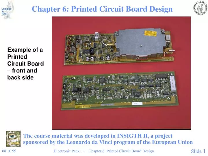
Chapter 6: Printed Circuit Board Design. Example of a Printed Circuit Board – front and back side. The course material was developed in INSIGTH II, a project sponsored by the Leonardo da Vinci program of the European Union. PCB Design, Introduction.

E N D
Chapter 6: Printed Circuit Board Design Example of a Printed Circuit Board – front and back side The course material was developed in INSIGTH II, a project sponsored by the Leonardo da Vinci program of the European Union Electronic Pack….. Chapter 6: Printed Circuit Board Design
PCB Design, Introduction • For new electronic products, designers are key persons, but should work in intimate cooperation with: • Sales, marketing and customers • Subcontractors • Production process experts • Cost engineers • Logistics and purchasing staff • etc. Electronic Pack….. Chapter 6: Printed Circuit Board Design
PCB Design, continued • Advanced PCB CAD tools a neccessity • Schematics • Component Library • Critical Parameters (Placement Constraints, Electromagnetic Compatibility, Thermal Limitations, etc) • Automatic Routing • Final Touch Manual Routing • (Verification by Final Simulation and Back Annotation) Electronic Pack….. Chapter 6: Printed Circuit Board Design
PCB CAD tools, continued • Output: • Final Schematics • Assembly Drawings • Documentation for PWB Manufacturer (”Gerber” file giving input for making PWB Manucturing Data (See Chapter 5): • Data for Photo- or Laser Plotter for Making Photographic Films and Printing Masks • Data for Numeric Drilling and Milling Machines • Data for Placement Machines • Data for Test Fixtures and Testing Machines Electronic Pack….. Chapter 6: Printed Circuit Board Design
PCB Design, continued • Guidelines for Right Quality • Choice of Best Suited Technology/Technologies • Choice of Components: Right Compromise between Performance, Reliability, Cost, etc. • Design for Production • Design for Testability • Design for Repair Electronic Pack….. Chapter 6: Printed Circuit Board Design
PCB Design, continued • Guidelines on Design for Manufacture • Few layers • Coarse pattern • Standardisation • Robust design (coarse tolerances) • Orderly placement Fig. 6.1.a: Proper component placement for hole- and surface mounted components Electronic Pack….. Chapter 6: Printed Circuit Board Design
Orderly Placement, continued Fig. 6.1.b: Proper component placement for hole- and surface mounted IC components Electronic Pack….. Chapter 6: Printed Circuit Board Design
PCB Design, continued • Important Guideline for "Robust Design": • Circuits should function with large parameter tolerances: • Design windows allowing for variations in component parameters. • Process windows allowing for variations in each process step. • Regulatory requirements on safety and EMC should be passed within the specified design and process windows. Electronic Pack….. Chapter 6: Printed Circuit Board Design
Design of Hole and Surface Mounted PCBs: Design Parameters • Minimum Dimensions: • The conductor cross section areas and resistivity of the material determine maximum current capacity and thereby minimum dimensions. • Current capacity is limited by excessive heating of the conductors and the PCB. • Maximum allowed ohmic voltage drop along the conductor also determines minimum dimensions. Electronic Pack….. Chapter 6: Printed Circuit Board Design
Design Parameters: Minimum Dimensions Fig. 6.2: Current capacity and temperature increase in conductors on PCBs.The upper figure shows the temperature increase (labels on each curve) at different combinations of cross-sections and currents). The lower figure shows the conductor cross-section (along the x-axis) as a function of the conductor width for different Cu-layer thicknesses. Electronic Pack….. Chapter 6: Printed Circuit Board Design
Design Parameters: DC Line Resistance: • DC Line resistance:R = r • L/(t • b)r ~ 2 .0 • 10 -8Wm for Cu foil • r is resistivity of the conductor material (ohm m) • L is conductor length • t is conductor thickness • b is conductor width • Sheet Resistance[ohm/square]: • Rsq = r / t • R = Rsq • L / b • 18 um copper: Rsq~ 1 mW/sq • 35 um copper: Rsq~ 0.5 mW/sq L b t Current I L r/ R = R • R = t b Electronic Pack….. Chapter 6: Printed Circuit Board Design
Hole and Surface Mounted PCB Design • Pattern Minimum Dimensions: Table 6.1: Examples of minimum dimension and PCB classes. The class indicates how many conductors can pass between the solder pads of a DIP package (no. of channels), and typical corresponding minimum dimensions in mm. When two figures are given for hole diameters, they are for component- and via holes respectively. Electronic Pack….. Chapter 6: Printed Circuit Board Design
Pattern Minimum Dimensions,continued a) b) Fig. 6.4: a): Parameters in layout dimensions used in Table 6.1. b): Minimum dimensions for solder mask for surface mount PWBs. Left: Dimensions for screen printed solder mask, with one common opening for all solder lands of an IC package. Right: Photoprocessible solder mask with a "pocket" for each terminal, permitting conductors between the solder lands. Electronic Pack….. Chapter 6: Printed Circuit Board Design
Mixed Hole Mount and SMD Printed Circuit Boards • Mixed PCBs are quite common due to: • Technical issues • Component availability and cost • Available capacity and performance of equipment in PCB manufacturing line(s). Fig. 6.5: Common types of SMD- and mixed SMD-/hole mount PCBs. Electronic Pack….. Chapter 6: Printed Circuit Board Design
SMD Printed Circuit Boards • Important aspects of design: • Component heat tolerances for reflow-/wave solder processes • Component orientation for wave solder: • Shadowing • Solder thieves for wave soldering • Minimum distance between components • Isolated via holes/solder lands Fig. 6.6: Preferred and not preferred directions of SMD components during wave soldering. Electronic Pack….. Chapter 6: Printed Circuit Board Design
Important Aspects of Design, continued Fig. 6.7: Minimum separation between SMD components during wave soldering. Electronic Pack….. Chapter 6: Printed Circuit Board Design
Important Aspects of Design, continued Fig. 6.8: Solder lands for SMD components should be separated from heavy copper areas by narrow constrictions. Conductors should preferably leave the solder lands of one component symmetrically. Electronic Pack….. Chapter 6: Printed Circuit Board Design
Important Aspects of Design, continued Fig. 6.9: Via holes should be separated from solder lands. Electronic Pack….. Chapter 6: Printed Circuit Board Design
Important Aspects of Design, continued Fig. 6.10: Dummy land for better control of the amount of adhesive in wave soldering process. Electronic Pack….. Chapter 6: Printed Circuit Board Design
Important Aspects of Design, continued Fig. 6.11: "Solder thieves" are areas in the Cu layer to reduce bridging in wave soldering. Electronic Pack….. Chapter 6: Printed Circuit Board Design
Important Aspects of Design, continued Fig. 6.12: Parameters defining solder land dimensions for SMD resistors and capacitors, please refer to Table 6.2. Electronic Pack….. Chapter 6: Printed Circuit Board Design
Solder Land Dimensions Table 6.2: Solder land dimensions for SMD resistors and capacitors (mm), please refer to Figure 6.12. Electronic Pack….. Chapter 6: Printed Circuit Board Design
Solder Land Dimensions, continued Fig. 6.13: Additional dimensions of SMD component and solder lands. Width a: a = Wmax + K Length b: * Reflow : b = Hmax + 2Tmax + K * Wave: b = Hmax + 2Tmax + 2K Length B: B = Lmax + 2Hmax + 2Tmax + K, K = 0.25 mm. Electronic Pack….. Chapter 6: Printed Circuit Board Design
Solder Land Dimensions, continued Fig. 6.14: Solder land dimensions for SMD transistors and diodes. Electronic Pack….. Chapter 6: Printed Circuit Board Design
Solder Land Dimensions, continued Table 6.3: Solder land dimensions for SO or VSO components (mm), please refer to Figure 6.15. Fig. 6.15: Solder land dimensions for SO and VSO packages, please refer to Table 6.3. Electronic Pack….. Chapter 6: Printed Circuit Board Design
Solder Land Dimensions, continued Fig. 6.16: Solder land dimensions for PLCC, LLCC and flatpacks, please refer to Tables 6.4 - 6.7. • a = Bmax + 0.1 mm B = width of leas • b = Fmax + 0.4 mm F = length of lead footprint • A,B = Emax + 0.8 mm E = separation between lead ends Electronic Pack….. Chapter 6: Printed Circuit Board Design
Solder Land Dimensions, continued Table 6.4: Solder land dimensions for PLCC (mm), please refer to Figure 6.16. Pitch, P = 1.27 (0.050") a = 0.63 b = 2.0 Table 6.5: Solder land dimensions for LLCC (mm), please refer to Figure 6.16. Pitch, P = 1.27 (0.050") a = 0.63 b = 2.5 Electronic Pack….. Chapter 6: Printed Circuit Board Design
Solder Land Dimensions, continued Table 6.6: Solder land dimensions for flatpacks (mm), please refer to Figure 6.16. b = 2.5 Electronic Pack….. Chapter 6: Printed Circuit Board Design
Solder Land Dimensions, continued Fig. 6.17: Solder land dimensions for TAB. Electronic Pack….. Chapter 6: Printed Circuit Board Design
Design for Testability Fig. 6.18: a): Correct position of test point, separated from solder land. b): Test points on solder lands are not recommended. c): Testing on components or component leads should be avoided. Electronic Pack….. Chapter 6: Printed Circuit Board Design
Design for Testability, continued Fig. 6.19: Examples of test point placement on a grid with 0.1” spacing, for testing of SMD components with 0.05” pitch. Electronic Pack….. Chapter 6: Printed Circuit Board Design
Testability • Defect level: • DL (ppm) = 1 - Y(1-T) x 106 • DL = defect level • Y = yield • T = fault coverage • Test Methods • Functional test • In-circuit test • Scan path • Boundary scan • Built-in self test Electronic Pack….. Chapter 6: Printed Circuit Board Design
Test Principles • Guidelines for Test Strategy • Single sided (normally) - double sided test fixtures are expensive and less robust • Separate test points - avoid using component leads or solder lands • 0.1" grid (normally) - 0.05 ” test probes are fragile • Solder on test points for reliable contact • Watch out and consider possible problems with high components Electronic Pack….. Chapter 6: Printed Circuit Board Design
Material Considerations for Thermal Compatibility Fig. 6.20: Mechanical strain is caused by difference in coefficient of thermal expansion (TCE), and changes in temperature. The magnitude of the corresponding stress depends on dimensions, temperature difference/change, and the elastic moduli of the materials. Electronic Pack….. Chapter 6: Printed Circuit Board Design
Thermal Design Fig. 6.21: a): Heat flow from hole mounted and surface mounted components on a PCB. b): Relative amount of heat removed by conduction, convection and radiation, from DIP hole mounted components and SMD LLCC components - typical values. Electronic Pack….. Chapter 6: Printed Circuit Board Design
Thermal Design • Fourier´s law • Q = DT/RT • RT = (1/K) • (L/A) Q = Heat flow [W] DT = Temperature difference [°C] RT = Thermal resistance [°C/W] K = Thermal conductivity [W/m°C] L,A = Length / cross-section • Equivalent to Ohm´s law : • I = DU/Rel Rel = 1/s • L/A • Convection: Q = h • A • DT • h = convection coefficient [W/m oC] • Fig. 6.22: • a): Heat flow due to conduction - Fourier´s equation. • b): Heat flow due to convection. Electronic Pack….. Chapter 6: Printed Circuit Board Design
Thermal Design, continued • Thermal Resistance • Rjc: Thermal resistance junction - case • Rjl: Thermal resistance junction - lead • Rja:Thermal resistance junction - ambient • Tj = Ta + P • Rja • Ta: Ambient temperature • Tj : Junction temperature Fig. 6.23: Thermal model of an IC and package. Electronic Pack….. Chapter 6: Printed Circuit Board Design
Thermal Design, continued • Example: IBM’s Thermal Module for Mainframe Logics Electronic Pack….. Chapter 6: Printed Circuit Board Design
Thermal Design, continued Table 6.8: Typical thermal resistances for various package types [oC/W] Electronic Pack….. Chapter 6: Printed Circuit Board Design
Thermal Design, continued Table 6.9: Typical values for the effective thermal conductivity of different types of PCBs. Electronic Pack….. Chapter 6: Printed Circuit Board Design
Thermal Design, continued • Effective Thermal Conductivity in PCBs • Keff = S (kiti) / ttot • ki = thermal conductivity layer i • ti = thickness layer i • ttot = total thickness Electronic Pack….. Chapter 6: Printed Circuit Board Design
Thermal Design, continued • Design of Right Thermal Coefficient of Expansion (TCE) • a = S ( ai Ei ti ) / S ( Ei ti ) • ti = thickness of layer i • ai = TCE material in layer i • Ei = Elastic modulus of layer i Table 6.10: Material parameters for calculating TCE and effective thermal conductivity of metal core boards. Electronic Pack….. Chapter 6: Printed Circuit Board Design gp-Untis 2003/0 VÅR 2004 - Termin 3 og 4 HØGSKOLEN I VESTFOLD 09.01.04 09.25 2 MT22.år Bachelor Mikroteknologi :::::::::DET TAS FORBEHOLD OM ENDRINGER
Thermal Design, continued Fig. 6.24: Cross section and thicknesses for a practical PWB with two Cu/Invar/Cu cores. The thicknesses were designed to get an over-all TCE of 7.5 [ppm/°C • m] The achieved value was measured to be 9.3 [ppm/°C • m] Calculated effective thermal conductivity in the x - y directions was 21 [W/ °C • m] Electronic Pack….. Chapter 6: Printed Circuit Board Design
Thermal Design, continued Fig. 6.25: a): Pin-grid package with cooling fins. b): Measured thermal resistance in the component with forced air cooling. Electronic Pack….. Chapter 6: Printed Circuit Board Design
Thermal Design, continued Fig. 6.26: LLCC package with thermal solder lands and thermal vias connected to a metal core in the PCB. Electronic Pack….. Chapter 6: Printed Circuit Board Design
Thermal Design, continued • Improved Cooling • Thermal vias • Cooling fins • Fan • Thermally conducting gas: helium, fluorocarbon • Liquid: water, fluorocarbon, oil • Boiling liquid • Heat pipe • Impingement cooling • Microbellows • Microgrooves Electronic Pack….. Chapter 6: Printed Circuit Board Design
Thermal Design, continued Fig. 6.27: a): Forced air convection in a channel between two PCBs (Texas Instruments) b): water-cooled heat exchanger for edge cooling of PCBs and temperature distribution (qualitative). Electronic Pack….. Chapter 6: Printed Circuit Board Design
Thermal Design, continued Fig. 6.28: Heat convection coefficient in different cooling media for natural convection, forced convection and boiling Electronic Pack….. Chapter 6: Printed Circuit Board Design
Thermal Design, continued Fig. 6.29: "Microbellows cooling": A jet of water or other cooling liquid impinges on the backside of the chip. The bellow structure is necessary to accommodate thermal expansion Electronic Pack….. Chapter 6: Printed Circuit Board Design
Thermal Design, continued Fig. 6.30: Cooling by forcing liquid through microscopic, etched channels in the semiconductor chip [6.32]. The channels are approximately 400 µm deep and 100 µm wide. Electronic Pack….. Chapter 6: Printed Circuit Board Design