Download
1 / 19
240 likes | 324 Views
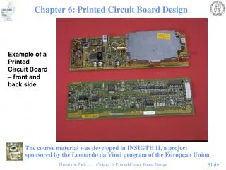
Printed Circuit Board Design. Avnish Kumar Dept. of Electrical & Computer Engineering University of Connecticut September 26, 2016. (Based on Prof. Sung Y. Park’s slides, Fall 2014). Printed Circuit Board ?.

E N D
Printed Circuit Board Design Avnish Kumar Dept. of Electrical & Computer Engineering University of Connecticut September 26, 2016 (Based on Prof. Sung Y. Park’s slides, Fall 2014)
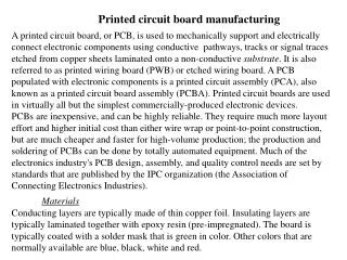
Printed Circuit Board ? • A printed circuit board (PCB) mechanically supports and electrically connects the electronic components using conductive tracks, pads and other features etched from copper sheets laminated onto a non-conductive substrate. • PCBs can be single sided (one copper layer), double sided (two copper layers) or multi-layer. • Conductors on different layers are connected with plated-through holes called Vias. • Advanced PCBs may contain components - capacitors, resistors or active devices - embedded in the substrate. 4
Multi-layer PCB design • 2 Layer PCB design: Top layer and bottom layer • 4 Layer PCB design: Top, Bottom, and two middle layers. 3
Three Elements to be considered • Components : - How to select components? - What values are needed? - What kind of package will be available/are needed? • Printed Circuit Board : - Schematic Design - PCB Layout Design - Prototype board • Case or Box for the prototype board : - Purchase or build by yourself 4
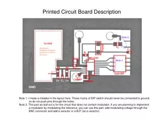
Printed Circuit Board Design Schematic Design 5 PCB Layout
Printed Circuit Board Design A PCB as a design on a computer (left) and realized as a board assembly populated with components (right). The board is double sided, with through-hole plating, green solder resist and a white legend. Both surface mount and through-hole components have been used. 6
Key Elements of a PCB • Pads are where the components are soldered to the PCB. • Traces are the copper tracks that connect pads together. • Via are small holes through the board that link a bottom and top trace together electrically. Traces on the same layer cannot cross, so often, when you are laying out a PCB, you need to jump from one layer to another. 7
Key Elements of a PCB • Silk-screen refers to any lettering that will appear on the final board. • Solder-mask is a layer of insulating lacquer that covers both sides of the board except where there are pads. 8
PCB design procedure • {Specific/Measurable} goals Design specification • Circuit diagram • Schematic design Select components Check the dimension Build a footprint Make a PCB library Add parts • Export schematic design to layout design • Route all connection • Design rule check • Generate Gerber files and drill file and zip them • Upload zip file to PCB order website 9
PCB Library design • Component datasheet • Dimension: mil (imperial unit) vs mm (metric) 1 inch =1000 mil, 1 mil = 0.0254 mm 1 mm = 39.3700787 mil DIP component and connector: 100 mil or 2.54 mm • Symbol in schematic vs Exact dimension in Layout • Pad number should be matched in schematic symbol and layout footprint 10
PCB Library dimension example • Male header 11
Tips for PCB design • Keep traces straight, • Try to avoid 90o turns use two 45o’s. • Double, even triple check layout, • Having a fresh pair of eyes look it over, • “measure twice, cut once” idea. • Trace thickness & spacing • Spacing of at least .010”, • 0.030” for In-house • ~0.025” per 1 Amp carrying lines, • Don’t use anything smaller than 0.010” for traces, • 0.030” for In-house milling. • Try to keep all connections on one side of PCB • Take into account component package 12
Tips for PCB design • Keep traces straight • Try to avoid 90˚ turns, use two 45˚ turns instead • Double (even triple) check the layout • Have a fresh pair of eyes look over it • “measure twice, cut once” idea • Trace thickness & spacing • Spacing of atleast 0.01 inches; 0.03 inches for In-house • ~0.025 inches per 1 Amp carrying lines • Don’t use anything smaller than 0.01 inches for traces; 0.03 inches for In-house • Try to keep all connections on one side of the PCB • Take into account the component packages 13
Free PCB design program • EAGLE • Cross-platform, Free with limitations, upgrades from $70 – $1640. A powerhouse in the hobbyist world, EAGLE probably has the most community support. • KiCad • Free and open source, no limitations • Express PCB • Free, no limitations. ExpressPCB is backed by ExpressPCBso this makes it very easy to send your design for manufacture. • DesignSpark PCB • Free, no limitations 14
Making PCBs • Layout your circuit / circuits • Check out http://www.expressPCB.com for some great tips on component layout and power distribution. • Layout is more of an art. • Tight spaces • Lots of connections • Make a 2 level board into a 3 level with vias 15
PCB Design Assignment • Every senior deign team needs to design one PCB during the fall semester • The number of components used should be more than 5 (connectors, surface mount components, through-hole components, ICS etc.) • The number of layers should be 2 or more • Report due date is November 19th 2016 • Report should contain: Schematic, layout design, and free DFM check result† of the PCB. † https://www.my4pcb.com/net35/FreeDFMNet/FreeDFMHome.aspx 19