Download
1 / 50
500 likes | 640 Views
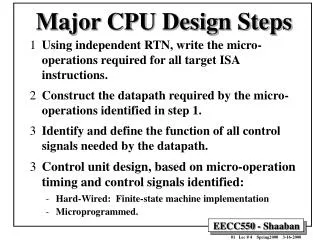
Major CPU Design Steps. 1. Analyze instruction set operations using independent RTN ISA => RTN => datapath requirements. This provides the the required datapath components and how they are connected to meet ISA requirements.

E N D
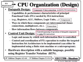
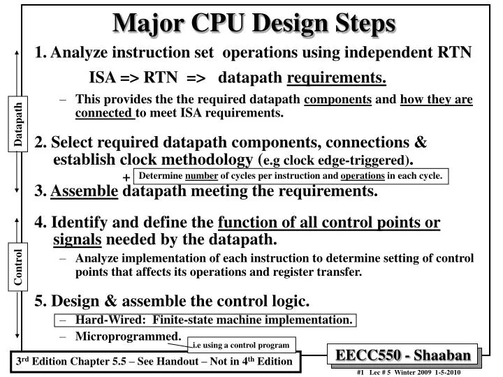
Major CPU Design Steps 1. Analyze instruction set operations using independent RTN ISA => RTN => datapath requirements. • This provides the the required datapath components and how they are connected to meet ISA requirements. 2. Select required datapath components, connections & establish clock methodology (e.g clock edge-triggered). 3. Assemble datapath meeting the requirements. 4. Identify and define the function of all control points or signals needed by the datapath. • Analyze implementation of each instruction to determine setting of control points that affects its operations and register transfer. 5. Design & assemble the control logic. • Hard-Wired: Finite-state machine implementation. • Microprogrammed. Datapath + Determine number of cycles per instruction and operations in each cycle. Control i.e using a control program 3rd Edition Chapter 5.5 – See Handout – Not in 4th Edition
Instruction<31:0> Inst Memory <0:15> <21:25> <16:20> <11:15> ALUop (2-bits) ALU Control Adr Rs Rt Rd Imm16 Branch PCSrc Zero RegDst MemWr MemtoReg Function Field Zero Rt Rd 0 1 Rs Rt 4 PC+4 RegWr 5 5 5 Main ALU R[rs] busA Rw Ra Rb = 0 busW 00 Adder 32 32 32-bit Registers R[rt] ALU 0 32 busB 32 0 PC Mux 32 Mux Mux 1 Clk 32 WrEn Adr 1 Clk 1 Data In Adder Data Memory Extender imm16 PC Ext 32 Branch Target 16 imm16 Clk ExtOp ALUSrc (Includes ORI not in book version) Single Cycle MIPS Datapath: CPI = 1, Long Clock Cycle T = I x CPI x C Jump Not Included
32 32 32 32 32 32 Single Cycle MIPS Datapath Extended To Handle Jump with Control Unit Added PC +4 PC +4 PC +4 Branch Target Book figure may have an error! Opcode rs R[rs] rt R[rt] rd R[rt] imm16 ALUOp (2-bits) 00 = add 01 = subtract 10 = R-Type Function Field Figure 5.24 page 314 In this book version, ORI is not supported—no zero extend of immediate needed.
Drawbacks of Single-Cycle Processor CPI = 1 • Long cycle time: • All instructions must take as much time as the slowest: • Cycle time for load is longer than needed for all other instructions. • Real memory is not as well-behaved as idealized memory • Cannot always complete data access in one (short) cycle. • Impossible to implement complex, variable-length instructions and complex addressing modes in a single cycle. • e.g indirect memory addressing. • High and duplicate hardware resource requirements • Any hardware functional unit cannot be used more than once in a single cycle (e.g. ALUs). • Cannot pipeline (overlap) the processing of one instruction with the previous instructions. • (instruction pipelining, chapter 6).
Main Control op ALU control fun ALUSrc Branch, Jump Equal ExtOp MemRd MemWr MemWr RegWr RegDst ALUctr Reg. Wrt ALU Register Fetch Ext Mem Access PC Instruction Fetch Next PC Result Store Data Mem Abstract View of Single Cycle CPU 1 ns 2 ns 1 ns 2 ns 2 ns One CPU Clock Cycle Duration C = 8ns One instruction per cycle CPI = 1 • Assuming the following datapath/control hardware components delays: • Memory Units: 2 ns ALU and adders: 2 ns • Register File: 1 ns Control Unit < 1 ns
Arithmetic & Logical PC Inst Memory Reg File ALU setup mux mux Load PC Inst Memory Reg File ALU Data Mem setup mux mux Critical Path Store PC Inst Memory Reg File ALU Data Mem mux Branch PC Inst Memory Reg File cmp mux Single Cycle Instruction Timing (Determines CPU clock cycle, C) Critical Path: Load (e.g 8 ns)
Clk . . . . . . . . . . . . Clock Cycle Time & Critical Path One CPU Clock Cycle Duration C = 8ns here • Critical path: the slowest path between any two storage devices • Clock Cycle time is a function of the critical path, and must be greater than: • Clock-to-Q + Longest Delay Path through the Combination Logic + Setup + Clock Skew Critical Path i.e longest delay LW in this case • Assuming the following datapath/control hardware components delays: • Memory Units: 2 ns ALU and adders: 2 ns • Register File: 1 ns Control Unit < 1 ns
Reducing Cycle Time: Multi-Cycle Design • Cut combinational dependency graph by inserting registers / latches. • The same work is done in two or more shorter cycles, rather than one long cycle. storage element storage element Two shorter cycles Acyclic Combinational Logic (A) One long cycle Cycle 1 Acyclic Combinational Logic e.g CPI =1 e.g CPI =2 => storage element Storage Element: Register or memory Acyclic Combinational Logic (B) Cycle 2 storage element • Place registers to: • Get a balanced clock cycle length • Save any results needed for the remaining cycles storage element
Instruction Fetch Next Instruction Instruction Decode Execute Result Store Basic MIPS Instruction Processing Steps Instruction Memory } Obtain instruction from program storage Instruction ¬ Mem[PC] Common steps for all instructions Update program counter to address of next instruction PC ¬ PC + 4 Determine instruction type Obtain operands from registers Done by Control Unit Compute result value or status Store result in register/memory if needed (usually called Write Back).
Partitioning The Single Cycle Datapath Add registers between steps to break into cycles 1 ns 2 ns To Control Unit 2 ns Branch, Jump 1 ns MemWr MemWr MemRd RegWr RegDst ExtOp 2 ns ALUSrc ALUctr Reg. File Exec Operand Fetch Instruction Fetch Mem Access PC Next PC Result Store Data Mem Data Memory Access Cycle (MEM) Instruction Fetch Cycle (IF) Instruction Decode Cycle (ID) Execution Cycle (EX) Write back Cycle (WB) 1 2 3 4 5 • Place registers to: • Get a balanced clock cycle length • Save any results needed for the remaining cycles
Example Multi-cycle Datapath To Control Unit Branch, Jump MemToReg RegWr RegDst MemWr MemRd ALUctr ExtOp ALUSrc Equal Reg. File Ext ALU A Reg File R Instruction Fetch PC IR Next PC B Mem Access M Instruction Fetch (IF) 2ns Data Mem Instruction Decode (ID) 1ns Execution (EX) 2ns Memory (MEM) 2ns Write Back (WB) 1ns 1 2 3 4 5 Registers added: All clock-edge triggered (not shown register write enable control lines) IR: Instruction register A, B: Two registers to hold operands read from register file. R: or ALUOut, holds the output of the main ALU M: or Memory data register (MDR) to hold data read from data memory CPU Clock Cycle Time: Worst cycle delay = C = 2ns (ignoring MUX, CLK-Q delays) • Assuming the following datapath/control hardware components delays: • Memory Units: 2 ns ALU and adders: 2 ns • Register File: 1 ns Control Unit < 1 ns Thus Clock Rate: f = 1 / 2ns = 500 MHz
Operations (Dependant RTN) for Each Cycle Logic Immediate IR ¬ Mem[PC] A ¬ R[rs] B ¬ R[rt R ¬ A OR ZeroExt[imm16] R[rt] ¬ R PC ¬ PC + 4 Store IR ¬ Mem[PC] A ¬ R[rs] B ¬ R[rt] R ¬ A + SignEx(Im16) Mem[R] ¬ B PC ¬ PC + 4 Load IR ¬ Mem[PC] A ¬ R[rs] B ¬ R[rt R ¬ A + SignEx(Im16) M ¬ Mem[R] R[rt] ¬ M PC ¬ PC + 4 R-Type IR ¬ Mem[PC] A ¬ R[rs] B ¬ R[rt] R ¬ A funct B R[rd] ¬ R PC ¬ PC + 4 Branch IR ¬ Mem[PC] A ¬ R[rs] B ¬ R[rt] Zero ¬ A - B If Zero = 1: PC ¬ PC + 4 + (SignExt(imm16) x4) else (i.e Zero =0): PC ¬ PC + 4 Instruction Fetch IF ID EX MEM WB Instruction Decode Execution Memory Write Back Instruction Fetch (IF) & Instruction Decode cycles are common for all instructions
Cycle 1 Cycle 2 Cycle 3 Cycle 4 Cycle 5 Load IF ID EX MEM WB MIPS Multi-Cycle Datapath:Five Cycles of Load CPI = 5 • 1- Instruction Fetch (IF): • Fetch the instruction from instruction Memory. • 2- Instruction Decode (ID): • Operand Register Fetch and Instruction Decode. • 3- Execute (EX): Calculate the effective memory address. • 4- Memory (MEM): Read the data from the Data Memory. • 5- Write Back (WB): • Write the loaded data to the register file. Update PC.
Multi-cycle Datapath Instruction CPI • R-Type/Immediate: Require four cycles, CPI = 4 • IF, ID, EX, WB • Loads: Require five cycles, CPI = 5 • IF, ID, EX, MEM, WB • Stores: Require four cycles, CPI = 4 • IF, ID, EX, MEM • Branches/Jumps: Require three cycles, CPI = 3 • IF, ID, EX • Average or effective program CPI: 3 £ CPI £ 5 depending on program profile (instruction mix).
Cycle 1 Cycle 2 Clk Single Cycle Implementation: 8 ns Load Store Waste 2ns (500 MHz) Cycle 1 Cycle 2 Cycle 3 Cycle 4 Cycle 5 Cycle 6 Cycle 7 Cycle 8 Cycle 9 Cycle 10 Clk Multiple Cycle Implementation: IF ID EX MEM WB IF ID EX MEM IF Load Store R-type Single Cycle Vs. Multi-Cycle CPU 8ns (125 MHz) Multi-Cycle CPU: CPI = 3 to 5 C = 2ns One million instructions take from 106 x 3 x 2x10-9 = 6 msec to 106 x 5 x 2x10-9 = 10 msec depending on instruction mix used. Single-Cycle CPU: CPI = 1 C = 8ns One million instructions take = I x CPI x C = 106 x 1 x 8x10-9 = 8 msec f = 500 MHz f = 125 MHz T = I x CPI x C • Assuming the following datapath/control hardware components delays: • Memory Units: 2 ns ALU and adders: 2 ns • Register File: 1 ns Control Unit < 1 ns
inputs (opcode, conditions) Next State Logic Control State Output Logic outputs (control points) Control Unit Design: Finite State Machine (FSM) Control Model • State specifies control points (outputs) for Register Transfer. • Control points (outputs) are assumed to depend only on the current state and not inputs (i.e. Moore finite state machine) • Transfer (register/memory writes) and state transition occur upon exiting the state on the falling edge of the clock. Last State State X Current State Register Transfer Control Points e.g Flip-Flops State Transition Depends on Inputs Next State Moore Finite State Machine To datapath
“instruction fetch” IR ¬ MEM[PC] “decode / operand fetch” A ¬ R[rs] B ¬ R[rt] LW BEQ & Zero R-type ORi SW BEQ & ~Zero PC ¬ PC + 4+ SX || 00 PC ¬ PC + 4 Execute R ¬ A fun B R ¬ A or ZX R ¬ A + SX R ¬ A + SX M ¬ MEM[R] MEM[R] ¬ B PC ¬ PC + 4 Memory R[rd] ¬ R PC¬ PC + 4 R[rt] ¬ R PC ¬ PC + 4 R[rt] ¬ M PC ¬ PC + 4 Write-back Control Specification For Multi-cycle CPUFinite State Machine (FSM) - State Transition Diagram (Start state) To instruction fetch 13 states: 4 State Flip-Flops needed To instruction fetch To instruction fetch
Traditional FSM Controller next state Outputs control points state op cond Next State Logic Output Logic State Transition Table next State Inputs control points 11 Equal 6 Opcode Current State State 4 Outputs (Control points) op To datapath datapath State State register (4 Flip-Flops)
Traditional FSM Controller datapath + state diagram => control • Translate RTN statements into control points. • Assign states. • Implement the controller. More on FSM controller implementation in Appendix C
IR ¬ MEM[PC] 0000 “instruction fetch” imem_rd, IRen “decode / operand fetch” A ¬ R[rs] B ¬ R[rt] 0001 Aen, Ben ALUfun, Sen LW BEQ & Zero R-type ORi SW BEQ & ~Zero PC ¬ PC + 4+SX || 00 0010 R ¬ A + SX 1011 R ¬ A + SX 1000 R ¬ A fun B 0100 R ¬ A or ZX 0110 PC ¬ PC + 4 0011 Execute RegDst, RegWr, PCen M ¬ MEM[R] 1001 MEM[R] ¬ B PC ¬ PC + 4 1100 Memory R[rt] ¬ R PC ¬ PC + 4 0111 R[rd] ¬ R PC¬ PC + 4 0101 R[rt] ¬ M PC ¬ PC + 4 1010 Write-back Mapping RTNs To Control Points Examples& State Assignments 0 1 4 2 6 8 11 3 12 9 To instruction fetch state 0000 5 7 10 13 states: 4 State Flip-Flops needed To instruction fetch state 0000 To instruction fetch state 0000
Detailed Control Specification - State Transition Table IF Current Op field Z Next IR PC Ops Exec Mem Write-Back State en sel A B Ex Sr ALU S R W M M-R Wr Dst 0000 ?????? ? 0001 1 0001 BEQ 0 0011 1 1 0001 BEQ 1 0010 1 1 0001 R-type x 0100 1 1 0001 orI x 0110 1 1 0001 LW x 1000 1 1 0001 SW x 1011 1 1 0010 xxxxxx x 0000 1 1 0011 xxxxxx x 0000 1 0 0100 xxxxxx x 0101 0 1 fun 1 0101 xxxxxx x 0000 1 0 0 1 1 0110 xxxxxx x 0111 0 0 or 1 0111 xxxxxx x 0000 1 0 0 1 0 1000 xxxxxx x 1001 1 0 add 1 1001 xxxxxx x 1010 1 0 1 1010 xxxxxx x 0000 1 0 1 1 0 1011 xxxxxx x 1100 1 0 add 1 1100 xxxxxx x 0000 1 0 0 1 ID Can be combined in one state BEQ R ORI LW SW More on FSM controller implementation in Appendix C
32 0 Mux 0 Mux 1 Instruction Reg ALU Out 32 0 1 Mux 32 32 1 ALU Control Mux 1 0 Extend 16 4 << 2 Alternative Multiple Cycle Datapath (In Textbook) • Minimizes Hardware: 1 memory, 1 ALU PCWr PCWrCond PCSrc Zero ALUSrcA IorD MemWr IRWr RegDst RegWr 1 Mux 32 PC 0 PC Zero 32 Rs Ra 32 Address 5 32 Rt 32 Rb busA A ALU Ideal Memory 32 Reg File 5 Rt 0 Rw 32 32 B 32 Rd 1 Mem Data Reg Din Dout busW busB 2 32 3 MemRd Imm 32 ALUOp MemtoReg ALUSrcB
Alternative Multiple Cycle Datapath (In Textbook) rs rt rd imm16 i.e MDR • Shared instruction/data memory unit • A single ALU shared among instructions • Shared units require additional or widened multiplexors • Temporary registers to hold data between clock cycles of the instruction: • Additional registers: • Instruction Register (IR), Memory Data Register (MDR), A, B, ALUOut (Figure 5.27 page 322)
2 2 2 PC+ 4 PC rs Branch Target rt rd 32 32 32 32 32 32 32 imm16 (ORI not supported, Jump supported) Alternative Multiple Cycle Datapath With Control Lines(Fig 5.28 In Textbook) (Figure 5.28 page 323)
The Effect of The 1-bit Control Signals Signal Name RegDst RegWrite ALUSrcA MemRead MemWrite MemtoReg IorD IRWrite PCWrite PCWriteCond Effect when deasserted (=0) The register destination number for the write register comes from the rt field (instruction bits 20:16). None The first ALU operand is the PC None None The value fed to the register write data input comes from ALUOut register. The PC is used to supply the address to the memory unit. None None None Effect when asserted (=1) The register destination number for the write register comes from the rd field (instruction bits 15:11). The register on the write register input is written with the value on the Write data input. The First ALU operand is register A (i.e R[rs]) Content of memory specified by the address input are put on the memory data output. Memory contents specified by the address input is replaced by the value on the Write data input. The value fed to the register write data input comes from data memory register (MDR). The ALUOut register is used to supply the the address to the memory unit. The output of the memory is written into Instruction Register (IR) The PC is written; the source is controlled by PCSource The PC is written if the Zero output of the ALU is also active. (Figure 5.29 page 324)
The Effect of The 2-bit Control Signals Signal Name ALUOp ALUSrcB PCSource Value (Binary) 00 01 10 00 01 10 11 00 01 10 Effect The ALU performs an add operation The ALU performs a subtract operation The funct field of the instruction determines the ALU operation (R-Type) The second input of the ALU comes from register B The second input of the ALU is the constant 4 The second input of the ALU is the sign-extended 16-bit immediate (imm16) field of the instruction in IR The second input of the ALU is is the sign-extended 16-bit immediate field of IR shifted left 2 bits (for branches) Output of the ALU (PC+4) is sent to the PC for writing The content of ALUOut (the branch target address) is sent to the PC for writing The jump target address (IR[25:0] shifted left 2 bits and concatenated with PC+4[31:28] is sent to the PC for writing (i.e R[rs]) i.e jump address (Figure 5.29 page 324)
Operations (Dependant RTN) for Each Cycle Store IR ¬ Mem[PC] PC ¬ PC + 4 A ¬ R[rs] B ¬ R[rt] ALUout ¬ PC + (SignExt(imm16) x4) ALUout ¬ A + SignEx(Imm16) Mem[ALUout] ¬ B Jump IR ¬ Mem[PC] PC ¬ PC + 4 A ¬ R[rs] B ¬ R[rt] ALUout ¬ PC + (SignExt(imm16) x4) PC ¬ Jump Address Load IR ¬ Mem[PC] PC ¬ PC + 4 A ¬ R[rs] B ¬ R[rt] ALUout ¬ PC + (SignExt(imm16) x4) ALUout ¬ A + SignEx(Imm16) MDR ¬ Mem[ALUout] R[rt] ¬ MDR R-Type IR ¬ Mem[PC] PC ¬ PC + 4 A ¬ R[rs] B ¬ R[rt] ALUout ¬ PC + (SignExt(imm16) x4) ALUout ¬ A funct B R[rd] ¬ ALUout Branch IR ¬ Mem[PC] PC ¬ PC + 4 A ¬ R[rs] B ¬ R[rt] ALUout ¬ PC + (SignExt(imm16) x4) Zero ¬ A - B Zero: PC ¬ ALUout Instruction Fetch IF ID EX MEM WB Instruction Decode Execution Memory Write Back Instruction Fetch (IF) & Instruction Decode (ID) cycles are common for all instructions
High-Level View of Finite State Machine Control (Figure 5.32) 0-1 2-5 6-7 8 9 (Figure 5.34) (Figure 5.35) (Figure 5.36) (Figure 5.33) • First steps are independent of the instruction class • Then a series of sequences that depend on the instruction opcode • Then the control returns to fetch a new instruction. • Each box above represents one or several state. (Figure 5.31 page 332)
FSM State Transition Diagram (From Book) IF A ¬ R[rs] B ¬ R[rt] ALUout ¬ PC + (SignExt(imm16) x4) ID (Figure 5.38 page 339) IR ¬ Mem[PC] PC ¬ PC + 4 ALUout ¬ A + SignEx(Imm16) PC ¬ Jump Address EX ALUout ¬ A func B Zero ¬ A -B Zero: PC ¬ ALUout MDR ¬ Mem[ALUout] WB MEM R[rd] ¬ ALUout Mem[ALUout] ¬ B Total 10 states R[rt] ¬ MDR WB More on FSM controller implementation in Appendix C
Instruction Fetch (IF) and Decode (ID) FSM States A ¬ R[rs] B ¬ R[rt] ALUout ¬ PC + (SignExt(imm16) x4) IF ID IR ¬ Mem[PC] PC ¬ PC + 4 (Figure 5.33) (Figure 5.34) (Figure 5.35) (Figure 5.36) (Figure 5.32 page 333)
2 2 2 PC+ 4 PC rs Branch Target rt rd 32 32 32 32 32 32 32 imm16 (ORI not supported, Jump supported) Instruction Fetch (IF) Cycle (State 0) IR ¬ Mem[PC] PC ¬ PC + 4 MemRead = 1 ALUSrcA = 0 IorD = 0 IRWrite =1 ALUSrcB = 01 ALUOp = 00 (add) PCWrite = 1 PCSource = 00 00 1 1 0 1 01 1 0 00 Add (Figure 5.28 page 323)
2 2 2 PC+ 4 PC rs Branch Target rt rd 32 32 32 32 32 32 32 imm16 (ORI not supported, Jump supported) Instruction Decode (ID) Cycle (State 1) A ¬ R[rs] B ¬ R[rt] ALUout ¬ PC + (SignExt(imm16) x4) ALUSrcA = 0 ALUSrcB = 11 ALUOp = 00 (add) (Calculate branch target) 11 0 00 Add (Figure 5.28 page 323)
Load/Store Instructions FSM States (From Instruction Decode) EX ALUout ¬ A + SignEx(Imm16) i.e Effective address calculation MDR ¬ Mem[ALUout] Mem[ALUout] ¬ B MEM R[rt] ¬ MDR WB To Instruction Fetch (Figure 5.32) (Figure 5.33 page 334)
2 2 2 PC+ 4 PC rs Branch Target rt rd 32 32 32 32 32 32 32 imm16 (ORI not supported, Jump supported) Load/Store Execution (EX) Cycle (State 2) Effective address calculation ALUSrcA = 1 ALUSrcB = 10 ALUOp = 00 (add) ALUout ¬ A + SignEx(Imm16) 10 1 00 Add (Figure 5.28 page 323)
2 2 2 PC+ 4 PC rs Branch Target rt rd 32 32 32 32 32 32 32 imm16 (ORI not supported, Jump supported) Load Memory (MEM) Cycle (State 3) MDR ¬ Mem[ALUout] MemRead = 1 IorD = 1 1 1 (Figure 5.28 page 323)
2 2 2 PC+ 4 PC rs Branch Target rt rd 32 32 32 32 32 32 32 imm16 (ORI not supported, Jump supported) Load Write Back (WB) Cycle (State 4) RegWrite = 1 MemtoReg = 1 RegDst = 0 R[rt] ¬ MDR 1 0 1 (Figure 5.28 page 323)
2 2 2 PC+ 4 PC rs Branch Target rt rd 32 32 32 32 32 32 32 imm16 (ORI not supported, Jump supported) Store Memory (MEM) Cycle (State 5) Mem[ALUout] ¬ B MemWrite = 1 IorD = 1 1 1 (Figure 5.28 page 323)
(From Instruction Decode) R-Type Instructions FSM States EX ALUout ¬ A funct B WB R[rd] ¬ ALUout To State 0 (Instruction Fetch) (Figure 5.32) (Figure 5.34 page 335)
2 2 2 PC+ 4 PC rs Branch Target rt rd 32 32 32 32 32 32 32 imm16 (ORI not supported, Jump supported) R-Type Execution (EX) Cycle (State 6) ALUout ¬ A funct B ALUSrcA = 1 ALUSrcB = 00 ALUOp = 10 (R-Type) 00 1 10 R-Type (Figure 5.28 page 323)
2 2 2 PC+ 4 PC rs Branch Target rt rd 32 32 32 32 32 32 32 imm16 (ORI not supported, Jump supported) R-Type Write Back (WB) Cycle (State 7) R[rd] ¬ ALUout RegWrite = 1 MemtoReg = 0 RegDst = 1 1 1 0 (Figure 5.28 page 323)
Jump Instruction Single EX State Branch Instruction Single EX State (From Instruction Decode) (From Instruction Decode) Zero ¬ A - B Zero : PC ¬ ALUout PC ¬ Jump Address EX EX To State 0 (Instruction Fetch) (Figure 5.32) To State 0 (Instruction Fetch) (Figure 5.32) (Figures 5.35, 5.36 page 337)
2 2 2 PC+ 4 PC rs Branch Target rt rd 32 32 32 32 32 32 32 imm16 (ORI not supported, Jump supported) Branch Execution (EX) Cycle (State 8) Zero ¬ A - B Zero : PC ¬ ALUout ALUSrcA = 1 ALUSrcB = 00 ALUOp = 01 (Subtract) PCWriteCond = 1 PCSource = 01 1 01 00 1 01 Subtract (Figure 5.28 page 323)
2 2 2 PC+ 4 PC rs Branch Target rt rd 32 32 32 32 32 32 32 imm16 (ORI not supported, Jump supported) Jump Execution (EX) Cycle (State 9) PCWrite = 1 PCSource = 10 PC ¬ Jump Address 10 1 1 (Figure 5.28 page 323)
MIPS Multi-cycle Datapath Performance Evaluation • What is the average CPI? • State diagram gives CPI for each instruction type. • Workload (program) below gives frequency of each type. Type CPIi for type Frequency CPIi x freqIi Arith/Logic 4 40% 1.6 Load 5 30% 1.5 Store 4 10% 0.4 branch 3 20% 0.6 Average CPI: 4.1 Better than CPI = 5 if all instructions took the same number of clock cycles (5). T = I x CPI x C
Adding Support for swap to Multi Cycle Datapath • You are to add support for a new instruction, swap that exchanges the values of two registers to the MIPS multicycle datapath of Figure 5.28 on page 232 swap $rs, $rt • Swap used the R-Type format with: the value of field rs = the value of field rd • Add any necessary datapaths and control signals to the multicycle datapath. Find a solution that minimizes the number of clock cycles required for the new instruction without modifying the register file. Justify the need for the modifications, if any. • Show the necessary modifications to the multicycle control finite state machine of Figure 5.38 on page 339 when adding the swap instruction. For each new state added, provide the dependent RTN and active control signal values. R[rt] ¬ R[rs] R[rs] ¬ R[rt] i.e No additional register write ports
rs rt op rd [31-26] [25-21] [20-16] [10-6] 2 2 2 Adding swap Instruction Support to Multi Cycle Datapath We assume here rs = rd in instruction encoding Swap $rs, $rt R[rt] ¬ R[rs] R[rs] ¬ R[rt] PC+ 4 rs Branch Target R[rs] rt R[rt] rd imm16 The outputs of A and B should be connected to the multiplexor controlled by MemtoReg if one of the two fields (rs and rd) contains the name of one of the registers being swapped. The other register is specified by rt. The MemtoReg control signal becomes two bits.
Adding swap Instruction Support to Multi Cycle Datapath IF A ¬ R[rs] B ¬ R[rt] ALUout ¬ PC + (SignExt(imm16) x4) ID IR ¬ Mem[PC] PC ¬ PC + 4 EX ALUout ¬ A + SignEx(Imm16) WB1 R[rd] ¬ B ALUout ¬ A func B WB2 Zero ¬ A -B Zero: PC ¬ ALUout R[rt] ¬ A R[rd] ¬ ALUout MEM WB Swap takes 4 cycles WB
6 bits [31-26] 5 bits [25-21] 5 bits [20-16] 5 bits [15-11] 5 bits [4-0] 6 bits [10-5] add3 $s1 $s2 $s0 $s3 Not used OP rs rd rx rt Adding Support for add3 to Multi Cycle Datapath • You are to add support for a new instruction, add3, that adds the values of three registers, to the MIPS multicycle datapath of Figure 5.28 on page 232 For example: add3 $s0,$s1, $s2, $s3 Register $s0 gets the sum of $s1, $s2 and $s3. The instruction encoding uses a modified R-format, with an additional register specifier rx added replacing the five low bits of the “funct” field. • Add necessary datapath components, connections, and control signals to the multicycle datapath without modifying the register bank or adding additional ALUs. Find a solution that minimizes the number of clock cycles required for the new instruction. Justify the need for the modifications, if any. • Show the necessary modifications to the multicycle control finite state machine of Figure 5.38 on page 339 when adding the add3 instruction. For each new state added, provide the dependent RTN and active control signal values.
rs rt op rd [31-26] [25-21] [20-16] [10-6] [4-0] 2 2 rx add3 instruction support to Multi Cycle Datapath Add3 $rd, $rs, $rt, $rx R[rd] ¬ R[rs] + R[rt] + R[rx] rx is a new register specifier in field [0-4] of the instruction No additional register read ports or ALUs allowed Modified R-Format WriteB 2 PC+ 4 rs Branch Target rt rx rd imm16 1. ALUout is added as an extra input to first ALU operand MUX to use the previous ALU result as an input for the second addition. 2. A multiplexor should be added to select between rt and the new field rx containing register number of the 3rd operand (bits 4-0 for the instruction) for input for Read Register 2. This multiplexor will be controlled by a new one bit control signal called ReadSrc. 3. WriteB control line added to enable writing R[rx] to B
add3 instruction support to Multi Cycle Datapath IF A ¬ R[rs] B ¬ R[rt] ALUout ¬ PC + (SignExt(imm16) x4) ID IR ¬ Mem[PC] PC ¬ PC + 4 EX ALUout ¬ A + SignEx(Im16) WriteB EX1 ALUout ¬ A + B B ¬ R[rx] WriteB ALUout ¬ A func B EX2 Zero ¬ A -B Zero: PC ¬ ALUout ALUout ¬ ALUout + B R[rd] ¬ ALUout MEM WB Add3 takes 5 cycles WB