Download
1 / 66
660 likes | 761 Views
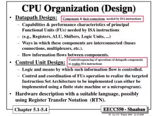
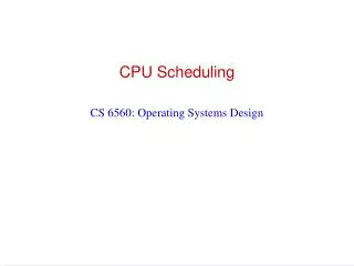
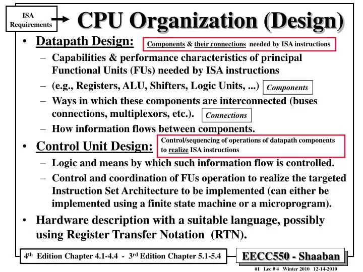
ISA Requirements. CPU Organization (Design). Components & their connections needed by ISA instructions. Datapath Design: Capabilities & performance characteristics of principal Functional Units (FUs) needed by ISA instructions (e.g., Registers, ALU, Shifters, Logic Units, ...)

E N D
ISA Requirements CPU Organization (Design) Components & their connections needed by ISA instructions • Datapath Design: • Capabilities & performance characteristics of principal Functional Units (FUs) needed by ISA instructions • (e.g., Registers, ALU, Shifters, Logic Units, ...) • Ways in which these components are interconnected (buses connections, multiplexors, etc.). • How information flows between components. • Control Unit Design: • Logic and means by which such information flow is controlled. • Control and coordination of FUs operation to realize the targeted Instruction Set Architecture to be implemented (can either be implemented using a finite state machine or a microprogram). • Hardware description with a suitable language, possibly using Register Transfer Notation (RTN). Components Connections Control/sequencing of operations of datapath components to realize ISA instructions 4th Edition Chapter 4.1-4.4 - 3rd Edition Chapter 5.1-5.4
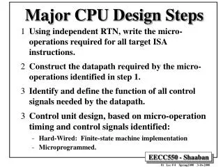
Major CPU Design Steps • Analyze instruction set to get datapath requirements: • Using independent RTN, write the micro-operations required for target ISA instructions. • This provides the the required datapath components and how they are connected. • Select set of datapath components and establish clocking methodology (defines when storage or state elements can read and when they can be written, e.g clock edge-triggered) • Assemble datapath meeting the requirements. • Identify and define the function of all control points or signals needed by the datapath. • Analyze implementation of each instruction to determine setting of control points that affects its operations. • Control unit design, based on micro-operation timing and control signals identified: • Combinational logic: For single cycle CPU. • Hard-Wired: Finite-state machine implementation. • Microprogrammed. 1 2 e.g Flip-Flops e.g Any instruction completed in one cycle i.e CPI = 1
ISA Requirements CPU Design CPU Design & Implantation Process • Top-down Design: • Specify component behavior from high-level requirements (ISA). • Bottom-up Design: • Assemble components in target technology to establish critical timing (hardware delays, critical path timing). • Iterative refinement: • Establish a partial solution, expand and improve. Instruction Set Architecture (ISA): Provides Requirements Processor Datapath Control Reg. File Mux ALU Reg Mem Decoder Sequencer Target VLSI implementation Technology Cells Gates
Datapath Design Steps • Write the micro-operation sequences required for a number of representative target ISA instructions using independent RTN. • Independent RTN statements specify: the required datapath components and how they are connected. • From the above, create an initial datapath by determining possible destinations for each data source (i.e registers, ALU). • This establishes connectivity requirements (data paths, or connections) for datapath components. • Whenever multiple sources are connected to a single input, a multiplexor of appropriate size is added. • Find the worst-time propagation delay in the datapath to determine the datapath clock cycle (CPU clock cycle, C). • Complete the micro-operation sequences for all remaining instructions adding datapath components + connections/multiplexors as needed. 1 2 (or destination)
31 26 21 16 11 6 0 op rs rt rd shamt funct 6 bits 5 bits 5 bits 5 bits 5 bits 6 bits 31 26 21 16 0 Immediate (imm16) op rs rt 6 bits 5 bits 5 bits 16 bits 31 26 0 op target address 6 bits 26 bits MIPS Instruction Formats R-Type • op: Opcode, operation of the instruction. • rs, rt, rd: The source and destination register specifiers. • shamt: Shift amount. • funct: Selects the variant of the operation in the “op” field. • address / immediate: Address offset or immediate value. • target address: Target address of the jump instruction. [31:26] [25:21] [20:16] [15:11] [10:6] [5:0] I-Type: ALU Load/Store, Branch Or address offset [31:26] [25:21] [20:16] [15:0] J-Type: Jumps [31:26] [25:0]
OP rs rd shamt funct rt 6 bits 5 bits 5 bits 5 bits 5 bits 6 bits MIPS R-Type (ALU) Instruction Fields R-Type: All ALU instructions that use three registers 1st operand 2nd operand Destination • op: Opcode, basic operation of the instruction. • For R-Type op = 0 • rs: The first register source operand. • rt: The second register source operand. • rd: The register destination operand. • shamt: Shift amount used in constant shift operations. • funct: Function, selects the specific variant of operation in the op field. Function Field Opcode for R-Type= 0 [31:26] [25:21] [20:16] [15:11] [10:6] [5:0] Rs, rt , rd are register specifier fields Independent RTN: Instruction Word ¬ Mem[PC] R[rd] ¬ R[rs] funct R[rt] PC ¬ PC + 4 Funct field value examples: Add = 32 Sub = 34 AND = 36 OR =37 NOR = 39 Operand register in rs Destination register in rd Operand register in rt add $1,$2,$3 sub $1,$2,$3 and $1,$2,$3 or $1,$2,$3 Examples: R-Type = Register Type Register Addressing used (Mode 1)
6 bits 5 bits 5 bits 16 bits Examples: add immediate: addi $1,$2,100 and immediate andi $1,$2,10 OP rs Immediate (imm16) rt MIPS ALU I-Type Instruction Fields I-Type ALU instructions that use two registers and an immediate value Loads/stores, conditional branches. • op: Opcode, operation of the instruction. • rs: The register source operand. • rt: The result destination register. • immediate: Constant second operand for ALU instruction. 1st operand Destination 2nd operand imm16 [31:26] [25:21] [20:16] [15:0] Independent RTN for addi: Instruction Word ¬ Mem[PC] R[rt] ¬ R[rs] + imm16 PC ¬ PC + 4 imm16 Source operand register in rs Result register in rt OP = 8 Constant operand in immediate OP = 12 I-Type = Immediate Type Immediate Addressing used (Mode 2) imm16 = 16 bit immediate field
6 bits 5 bits 5 bits 16 bits OP rs address rt MIPS Load/Store I-Type Instruction Fields Base Src./Dest. (e.g. offset) • op: Opcode, operation of the instruction. • For load word op = 35, for store word op = 43. • rs: The register containing memory base address. • rt: For loads, the destination register. For stores, the source register of value to be stored. • address: 16-bit memory address offset in bytes added to base register. imm16 [31:26] [25:21] [20:16] [15:0] Signed address offset in bytes Sign Extended imm16 base register in rs Examples: source register in rt Offset Instruction Word ¬ Mem[PC] Mem[R[rs] + imm16] ¬ R[rt] PC ¬ PC + 4 Store word: sw $3, 500($4) Load word: lw $1, 32($2) Instruction Word ¬ Mem[PC] R[rt] ¬ Mem[R[rs] + imm16] PC ¬ PC + 4 base register in rs Destination register in rt Offset Base or Displacement Addressing used (Mode 3) imm16 = 16 bit immediate field
Examples: Branch on equal beq $1,$2,100 Branch on not equal bne $1,$2,100 OP rs address rt MIPS Branch I-Type Instruction Fields (e.g. offset) • op: Opcode, operation of the instruction. • rs: The first register being compared • rt: The second register being compared. • address: 16-bit memory address branch target offset in words added to PC to form branch address. imm16 6 bits 5 bits 5 bits 16 bits [31:26] [25:21] [20:16] [15:0] Signed address offset in words Word = 4 bytes imm16 Register in rt offset in bytes equal to instruction address field x 4 Register in rs OP = 4 Imm16 x 4 Added to PC+4 to form branch target OP = 5 Independent RTN for beq: Sign extended Instruction Word ¬ Mem[PC] R[rs] = R[rt] : PC ¬ PC + 4 + imm16 x 4 R[rs] ¹ R[rt] : PC ¬ PC + 4 PC-Relative Addressing used (Mode 4) imm16 = 16 bit immediate field
OP jump target 6 bits 26 bits Examples: Jump j 10000 Jump and link jal 10000 0 0 jump target = 2500 4 bits 26 bits 2 bits MIPS J-Type Instruction Fields J-Type: Include jump j, jump and link jal • op: Opcode, operation of the instruction. • Jump j op = 2 • Jump and link jal op = 3 • jump target: jump memory address in words. Jump target in words [31:26] [25:0] Word = 4 bytes Jump memory address in bytes equal to instruction field jump target x 4 Effective 32-bit jump address: PC(31-28),jump_target,00 PC(31-28) From PC+4 Independent RTN for j: Instruction Word ¬ Mem[PC] PC ¬ PC + 4 PC ¬ PC(31-28),jump_target,00 J-Type = Jump Type Pseudodirect Addressing used (Mode 5)
31 26 21 16 11 6 0 op rs rt rd shamt funct 6 bits 5 bits 5 bits 5 bits 5 bits 6 bits 31 26 21 16 0 op rs rt Immediate (imm16) 6 bits 5 bits 5 bits 16 bits 31 26 21 16 0 op rs rt Immediate (imm16) 6 bits 5 bits 5 bits 16 bits 31 26 21 16 0 op rs rt Immediate (imm16) 6 bits 5 bits 5 bits 16 bits A Subset of MIPS Instructions 32 = add 34 = sub 0 ADD and SUB: add rd, rs, rt sub rd, rs, rt OR Immediate: ori rt, rs, imm16 LOAD and STORE Word lw rt, rs, imm16 sw rt, rs, imm16 BRANCH: beq rs, rt, imm16 R [31:26] [25:21] [20:16] [15:11] [10:6] [5:0] I 13 [31:26] [25:21] [20:16] [15:0] I Offset in bytes 35 = lw 43 = sw [31:26] [25:21] [20:16] [15:0] I Offset in words 4 [31:26] [25:21] [20:16] [15:0]
Instruction Fetch Next Instruction Instruction Decode Execute Result Store Basic MIPS Instruction Processing Steps Instruction Memory } Obtain instruction from program storage Instruction ¬ Mem[PC] Common steps for all instructions Update program counter to address of next instruction PC ¬ PC + 4 Determine instruction type Obtain operands from registers Done by Control Unit (Based on Opcode) Compute result value or status Store result in register/memory if needed (usually called Write Back). T = I x CPI x C
Common Steps Overview of MIPS Instruction Micro-operations • All instructions go through these common steps: • Send program counter to instruction memory and fetch the instruction. (fetch) Instruction ¬ Mem[PC] • Update the program counter to point to next instruction PC ¬ PC + 4 • Read one or two registers, using instruction fields. (decode) • Load reads one register only. • Additional instruction execution actions (execution) depend on the instruction in question, but similarities exist: • All instruction classes (except J type) use the ALU after reading the registers: • Memory reference instructions use it for effective address calculation. • Arithmetic and logic instructions (R-Type), use it for the specified operation. • Branches use it for comparison. • Additional execution steps where instruction classes differ: • Memory reference instructions: Access memory for a load or store. • Arithmetic and logic instructions: Write ALU result back in register. • Branch instructions: Possibly change next instruction address (update PC) based on comparison (i.e if branch is taken).
CPU Performance Equation: T = I x CPI x C 32 32 32 32 32 A Single Cycle MIPS CPU Design Design target: A single-cycle per instruction MIPS CPU design All micro-operations of an instruction are to be carried out in a single CPU clock cycle. Cycles Per Instruction = CPI = 1 Abstract view of single cycle MIPS CPU showing major functional units (components) and major connections between them CPI = 1 4th Edition Figure 4.1 page 302 - 3rd Edition Figure 5.1 page 287
OP rs rd shamt funct rt 6 bits 5 bits 5 bits 5 bits 5 bits 6 bits R-Type Example:Micro-Operation Sequence For ADD Instruction Word ¬ Mem[PC] Fetch the instruction PC ¬ PC + 4 Increment PC R[rd] ¬ R[rs] + R[rt] Add register rs to register rt result in register rd add rd, rs, rt 32 = add 34 = sub 0 0 [31:26] [25:21] [20:16] [15:11] [10:6] [5:0] Common Steps Program Memory i.e Funct =add = 32 Independent RTN ?
32 32 32 32 32 32 32 InstructionWord Initial Datapath Components Three components needed by: Instruction Fetch:Instruction ¬ Mem[PC] Program Counter Update:PC ¬ PC + 4 32-bit • Two state elements (memory) needed to store and access instructions: • Instruction memory: • Only read access (by user code). No read control signal needed. • Program counter (PC): 32-bit register. • Written at end of every clock cycle (edge-triggered) : No write control signal. • 32-bit Adder: To compute the the next instruction address (PC + 4). 4th Edition Figure 4.5, page 308 - 3rd Edition Figure 5.5, page 293 + Basics of logic design/logic building blocks review in Appendix C in Book CD (4th Edition Appendix B)
32 32 32 32 32 Building The Datapath Instruction Fetch & PC Update: 1 2 Instruction ¬ Mem[PC] PC ¬ PC + 4 2 PC ¬ PC + 4 1 Portion of the datapath used for fetching instructions and incrementing the program counter (PC). Instruction ¬Mem[PC] Clock input to PC, memory not shown PC write or update is edge triggered at the end of the cycle 4th Edition Figure 4.6 page 309 - 3rd Edition Figure 5.6 page 293
32 32 32 32 32 More Datapath Components ISA Register File e.g add = 0010 Main 32-bit ALU R[rs] (Function) R[rt] 32-bit Arithmetic and Logic Unit (ALU) • Register File: • Contains all ISA registers. • Two read ports and one write port. • Register writes by asserting write control signal • Clocking Methodology:Writes are edge-triggered. • Thus can read and write to the same register in the same clock cycle. Zero = Zero flag = 1 When ALU result equals zero 4th Edition Figure 4.7, page 310 - 3rd Edition Figure 5.7, page 295 + Basics of logic design/logic building blocks review in Appendix C in Book CD (4th Edition Appendix B)
RW RA RB Write Enable 5 5 5 busA busW 32 32 32-bit Registers 32 busB Clk 32 Register File Details • Register File consists of 32 registers: • Two 32-bit output busses: busA and busB • One 32-bit input bus: busW • Register is selected by: • RA (number) selects the register to put on busA (data): busA = R[RA] • RB (number) selects the register to put on busB (data): busB = R[RB] • RW (number) selects the register to be writtenvia busW (data) when Write Enable is 1 Write Enable: R[RW] ¬ busW • Clock input (CLK) • The CLK input is a factor ONLY during write operations. • During read operation, it behaves as a combinational logic block: • RA or RB valid => busA or busB valid after “access time.” Write Data
Register Write Enable (RegWrite) . . 32 0 1 . RW RA RB Write Enable 5 5 5 busA Write Write Write Write Data Out Data Out Data Out Data Out 32 Register 31 Register 0 Register 30 Register 1 busW . . . 32 32 32-bit Registers . 32 Data In Data In Data In Data In 32 busB Register Read Data 1 (Bus A) 0 Clk Write Register RW 32 . 32-to-1 MUX 32-to-1 MUX 1 . 30 31 . . . . 5 5-to-32 Decoder . . . . . . Read Register 1 (RA) . 32 30 0 1 31 . 32 5 . . . 32 32 Register Read Data 2 (Bus B) . 30 31 Register Write Data (Bus W) 5 Read Register 2 (RB) A Possible Register File Implementation Each Register contains 32 edge triggered D-Flip Flops 2 Read Ports Write Port R[rs] rd? rt? rs R[rt] Clock input to registers not shown in diagram rt Also see Appendix C in Book CD (3rd Edition Appendix B) - The Basics of Logic Design
Write Enable Address Data In DataOut 32 32 Clk Read Enable Idealized Memory • Memory (idealized) • One input bus: Data In. • One output bus: Data Out. • Memory word is selected by: • Address selects the word to put on Data Out bus. • Write Enable = 1: address selects the memoryword to be written via the Data In bus. • Clock input (CLK): • The CLK input is a factor ONLY during write operation, • During read operation, this memory behaves as a combinational logic block: • Address valid => Data Out valid after “access time.” • Ideal Memory = Short access time. Compared to other components in CPU datapath
. . . . . . . . . . . . Clocking Methodology Used:Edge Triggered Writes • All storage element (e.g Flip-Flops, Registers, Data Memory) writes are triggered by the same clock edge. • Cycle Time = CLK-to-Q + Longest Delay Path + Setup + Clock Skew Clk Setup Hold Setup Hold Don’t Care CLK-to-Q CLK-to-Q Critical Path (Longest delay path) Clock Clock Here writes are triggered on the rising edge of the clock
32 32 32 32 Simplified Datapath For MIPS R-Type Instructions rs 4 [25:21] [20:16] [15:11] From Instruction Memory (Function) R[rs] e.g add = 0010 rt rd R[rt] Components and connections as specified by RTN statement R[rd] ¬ R[rs] + R[rt] Clock input to register bank not shown i.e Funct = function =add Destination register R[rd] write or update is edge triggered at the end of the cycle
Function =Add, Subtract … 4 R[rs] Rd Rs Rt ALUctr RegWr 5 5 5 R[rt] busA Rw Ra Rb busW 32 32 32-bit Registers Result ALU 32 32 busB Clk 32 More Detailed Datapath For R-Type InstructionsWith Control Points Identified R[rd] ¬ R[rs] + R[rt] i.e Funct = function =add
Clk Clk-to-Q Old Value New Value PC Instruction Memory Access Time Rs, Rt, Rd, Op, Func Old Value New Value Delay through Control Logic ALUctr Old Value New Value RegWr Old Value New Value Register File Access Time busA, B Old Value New Value ALU Delay busW Old Value New Value Rd Rs Rt Register Write Occurs Here ALUctr RegWr 5 5 5 busA Rw Ra Rb busW 32 32 32-bit Registers Result ALU 32 32 busB Clk 32 R-Type Register-Register Timing PC+4 R[rs] All register writes occur on falling edge of clock (clocking methodology) R[rt]
31 26 21 16 0 op rs rt Immediate (imm16) 6 bits 5 bits 5 bits 16 bits Imm16 000 ….. 000 Logical Operations with Immediate Example:Micro-Operation Sequence For ORI Instruction Word ¬ Mem[PC] Fetch the instruction PC ¬ PC + 4 Increment PC R[rt] ¬ R[rs] OR ZeroExt[imm16] OR register rs with immediate field zero extended to 32 bits, result in register rt ori rt, rs, imm16 13 [31:26] [25:21] [20:16] [15:0] Done by Main ALU
1 0 Rd Rt RegDst Mux Rs Rt ALUctr RegWr 5 5 5 busA Rw Ra Rb busW 32 Result 32 32-bit Registers ALU 32 32 busB Clk 32 Mux ZeroExt imm16 32 16 ALUSrc Imm16 000 ….. 000 Datapath For Logical Instructions With Immediate 2x1 MUX (width 5 bits) Function = OR R[rs] R[rt] 0 2x1 MUX (width 32 bits) 1 R[rt] ¬ R[rs] OR ZeroExt[imm16]
31 26 21 16 0 op rs rt Immediate (imm16) 6 bits 5 bits 5 bits 16 bits Load Operations Example:Micro-Operation Sequence For LW Instruction Word ¬ Mem[PC] Fetch the instruction PC ¬ PC + 4 Increment PC R[rt] ¬ Mem[R[rs] + SignExt[imm16]] Immediate field sign extended to 32 bits and added to register rs to form memory load address, write word at load effective address to register rt lw rt, rs, imm16 35 Signed Address offset in bytes [31:26] [25:21] [20:16] [15:0] Instruction Memory Effective Address To load from Data Memory
32 32 32 For SignExt[imm16] Additional Datapath Components For Loads & Stores 4th Edition Figure 4.8, page 311 3rd Edition Figure 5.8, page 296 Inputs: for address and write (store) data Output for read (load) data 16-bit input sign-extended into a 32-bit value at the output Data memory write or update is edge triggered at the end of the cycle (clocking methodology)
Rd Rt RegDst 0 1 Mux Rs ALUctr RegWr 5 5 5 Base Address register MemtoReg R[rs] busA Rw Ra Rb Effective Address busW 32 32 32-bit Registers ALU 32 0 32 R[rt] busB Clk MemWr 0 32 Mux Mux WrEn Adr Offset Data In 1 32 1 Data Memory Extender 32 imm16 32 16 Clk ALUSrc ExtOp Datapath For Loads LW Function = add MemRd R[rt] ¬ Mem[R[rs] + SignExt[imm16]] Effective Address Data Memory
31 26 21 16 0 op rs rt Immediate (imm16) 6 bits 5 bits 5 bits 16 bits Store Operations Example:Micro-Operation Sequence For SW Instruction Word ¬ Mem[PC] Fetch the instruction PC ¬ PC + 4 Increment PC Mem[R[rs] + SignExt[imm16]] ¬ R[rt] Immediate field sign extended to 32 bits and added to register rs to form memory store effective address, register rt written to memory at store effective address. sw rt, rs, imm16 43 Signed Address offset in bytes [31:26] [25:21] [20:16] [15:0] Effective Address To store at Data Memory
Rd Rt MemtoReg ALUctr MemWr RegDst 0 1 Mux Rs Rt RegWr 5 5 5 Base Address register R[rs] busA Rw Ra Rb Effective Address busW 32 32 32-bit Registers ALU 0 32 32 R[rt] busB Clk 0 32 Mux Mux R[rt] WrEn Adr Offset Data In 32 1 32 Data Memory 1 Extender imm16 32 16 Clk ALUSrc ExtOp Datapath For Stores SW Add = MemRd Mem[R[rs] + SignExt[imm16]] ¬ R[rt] Effective Address Data Memory
31 26 21 16 0 op rs rt immediate 6 bits 5 bits 5 bits 16 bits Conditional Branch Example:Micro-Operation Sequence For BEQ Instruction Word ¬ Mem[PC] Fetch the instruction PC ¬ PC + 4 Increment PC Zero ¬ R[rs] - R[rt] Calculate the branch condition R[rs] == R[rt] (i.e R[rs] - R[rt] = 0 ) Zero : PC ¬ PC + ( SignExt(imm16) x 4 ) Calculate the next instruction’s PC address beq rs, rt, imm16 PC Offset in words 4 [31:26] [25:21] [20:16] [15:0] Condition Action Then Zero = 1 Branch Target “Zero” is zero flag of main ALU
Main ALU evaluates branch condition • New adder to compute branch target: • Sum of incremented PC and • sign-extended lower 16-bits on the • instruction. Datapath For Branch Instructions New 32-bit Adder (Third ALU) for Branch Target SignExt(imm16) x 4 PC + 4 + ( SignExt(imm16) x 4 [25:21] rs [20:16] rt = Subtract R[rs] R[rt] Zero flag =1 if R[rs] - R[rt] = 0 (i.e R[rs] = R[rt]) (Main ALU) [15:0] imm16 Main ALU EvaluatesBranch Condition(subtract) SignExt(imm16) 4th Edition Figure 4.9, page 312 - 3rd Edition Figure 5.9, page 297
32 Branch Zero Instruction Address Zero Rs Rt 32 PC+4 4 RegWr 5 5 5 0 00 busA Adder Rw Ra Rb busW 32 32 32-bit Registers Equal? PC Mux PC busB 1 Clk Main ALU (subtract) 32 imm16 Branch Target Adder PC Ext Clk New 2X1 32-bit MUX to select next PC value Branch Target ALU Sign extend shift left 2 More Detailed Datapath For Branch Operations R[rs] R[rt] New Third ALU (adder)
32 32 32 32 32 Combining The Datapaths For Memory Instructions and R-Type Instructions 4 [25:21]rs R[rs] [20:16]rt R[rt] 0 1 1 0 R[rt] rt/rd MUX not shown SignExt(imm16) [15:0] imm16 Highlighted muliplexors and connections added to combine the datapaths of memory and R-Type instructions into one datapath This is book version ORI not supported 4th Edition Figure 4.10 Page 314 - 3rd Edition Figure 5.10 Page 299
32 32 32 32 32 Instruction Fetch Datapath Added toALU R-Type and Memory Instructions Datapath PC+ 4 Combination of Figure 4.10 (p. 314) and Figure 4.6 (p. 309) [3rd Edition Figure 5.10 (p. 299) and Figure 5.6 (p. 293)] PC rs R[rs] rt R[rt] R[rt] rt/rd MUX not shown This is book version ORI not supported, no zero extend of immediate needed
Zero Branch PC +4 Branch Target 4 0 1 32 32 32 32 32 32 32 32 1 0 rt/rd MUX not shown A Simple Datapath For The MIPS Architecture • Datapath of branches and a program counter multiplexor are added. • Resulting datapath can execute in a single cycle the basic MIPS instruction: • - load/store word - ALU operations - Branches rs R[rs] rt R[rt] This is book version ORI not supported, no zero extend of immediate needed 4th Edition Figure 4.11 page 315 - 3rd Edition Figure 5.11 page 300
ALU Control Lines ALU Function 0000 AND 0001 OR 0010 add 0110 subtract 0111 Set-on-less-than 1100 NOR Main ALU Control 4th Edition Appendix C • The main ALU has four control lines (detailed design in Appendix B) with the following functions: • For our current subset of MIPS instructions only the top fivefunctions will be used (thus only three control lines will be used) • For R-type instruction the ALU function depends on both the opcode and the 6-bit “funct” function field • For other instructions the ALU function depends on the opcode only. • A local ALU control unit can be designed to accept 2-bit ALUop control lines (from main control unit) and the 6-bit function field and generate the correct 4-bit ALU control lines. Not Used Or 3 bits depending on number functions actually used
Instruction Opcode LW SW Branch Equal R-Type R-Type R-Type R-Type R-Type Instruction Operation Load word Store word branch equal add subtract AND OR set on less than ALUOp 00 00 01 10 10 10 10 10 Funct Field XXXXXX XXXXXX XXXXXX 100000 100010 100100 100101 101010 Desired ALU Action add add subtract add subtract and or set on less than ALU Control Lines 0010 0010 0110 0010 0110 0000 0001 0111 func ALUctr op 6 Main Control 4 ALU Control (Local) ALUop 6 2 ALU Local ALU Decoding of “func” Field Or 3 bits Opcode Subtract = 01 Add = 00 R-Type = 10
Local ALU Control Unit Add = 00 Subtract = 01 Add Subtract Add Subtract AND OR Set-On-less-Than { R-type =10 Page 302 (2 lines From main control unit) 2 Function Field 3 ALU Control Lines 4th line = 0 More details found in Appendix D in Book CD – (3rd Edition Appendix C)
Zero PC +4 Branch PC +4 Branch Target rs R[rs] rt R[rt] rd R[rt] 32 32 32 32 32 32 32 32 ALUOp (2-bits) 00 = add 01 = subtract 10 = R-Type imm16 Function Field Single Cycle MIPS Datapath Necessary multiplexors and control lines are identified here and local ALU control added: This is book version ORI not supported, no zero extend of immediate needed 4th Edition Figure 4.15 page 320 - 3rd Edition Figure 5.15 page 305
Inst Memory ALU Control Adr Branch Zero Adder Mux Adder Putting It All Together: A Single Cycle Datapath Instruction<31:0> <0:15> <21:25> <16:20> <11:15> ALUop (2-bits) 00 = add 01 = subtract 10 = R-Type Rs Rt Rd Imm16 PCSrc RegDst MemWr MemtoReg Function Field Zero Rt Rd 0 1 Rs Rt 4 PC+4 RegWr 5 5 5 Main ALU R[rs] busA Rw Ra Rb = 0 busW 00 32 32 32-bit Registers R[rt] ALU 0 32 busB 32 0 PC 32 Mux Mux 1 Clk 32 WrEn Adr 1 Clk 1 Data In Data Memory Extender imm16 PC Ext 32 Branch Target 16 imm16 Clk e.g Sign Extend + Shift Left 2 ExtOp ALUSrc MemRd (Includes ORI not in book version)
Instruction<31:0> Instruction Memory <21:25> <0:25> <21:25> <16:20> <11:15> <0:15> Adr Op Fun Jump_target Rt Rs Rd Imm16 Control Unit Control Lines ALOp (2-bits) Mem Write Mem Read MemtoReg Branch ALUSrc RegWrite RegDst DATA PATH
The Effect of The Control Signals Signal Name RegDst RegWrite ALUSrc Branch MemRead MemWrite MemtoReg Effect when deasserted (=0) The register destination number for the write register comes from the rt field (instruction bits 20:16). None The second main ALU operand comes from the second register file output (Read data 2) R[rt] The PC is replaced by the output of the adder that computes PC + 4 None None The value fed to the register write data input comes from the main ALU. Effect when asserted (=1) The register destination number for the write register comes from the rd field (instruction bits 15:11). The register on the write register input is written with the value on the Write data input. The second main ALU operand is the sign-extended lower 16 bits on the instruction (imm16) If Zero =1 The PC is replaced by the output of the adder that computes the branch target. Data memory contents designated by the address input are put on the Read data output. Data memory contents designated by the address input are replaced by the value on the Write data input. The value fed to the register write data input comes from data memory.
Instruction R-Format lw sw beq RegDst 1 0 X X ALUSrc 0 1 1 0 Memto- Reg 0 1 X X Reg Write 1 1 0 0 Mem Read 0 1 0 0 Mem Write 0 0 1 0 Branch 0 0 0 1 ALUOp1 1 0 0 0 ALUOp0 0 0 0 1 Control Line Settings Control Lines ALUOp (2-bits) 00 = add 01 = subtract 10 = R-Type 4th Edition Figure 4.18 page 323 3rd Edition Figure 5.18 page 308
The Truth Table For The Main Control (Opcode) Similar to Figure 4.22 Page 327 (3rd Edition Figure 5.22 Page 312)
PLA Implementation of the Main Control Control Lines Figure D.2.5 in Appendix D (3rd Edition Figure C.2.5 in Appendix C) PLA = Programmable Logic Array - Appendix C (3rd Edition Appendix B)
32 32 32 32 32 32 Single Cycle MIPS Datapath Control Unit Added PC +4 PC +4 PC +4 Branch Target Opcode rs R[rs] rt R[rt] rd imm16 ALUOp (2-bits) 00 = add 01 = subtract 10 = R-Type 4th Edition Figure 4.21, page 326 3rd Edition Figure 5.17, page 307 Function Field In this book version, ORI is not supported—no zero extend of immediate needed.
OP Jump_target 6 bits 26 bits 0 0 jump target 4 bits 26 bits 2 bits Adding Support For Jump:Micro-Operation Sequence For Jump: J Instruction Word ¬ Mem[PC] Fetch the instruction PC ¬ PC + 4 Increment PC PC ¬ PC(31-28),jump_target,00 Update PC with jump address j jump_target 2 Jump address in words [31:26] [25:0] PC(31-28) Jump Address 4 highest bits from PC + 4