Download
1 / 46
470 likes | 642 Views
Multi-Cycle Datapath. Lecture notes from MKP, H. H. Lee and S. Yalamanchili. Reading. Appendices B .7, D.3, D.4, D.5. Single Cycle Datapath. What are the performance limitations of this datapth ?. Why Multi-Cycle?. Single cycle datapath Design for the worst case

E N D
Multi-Cycle Datapath Lecture notes from MKP, H. H. Lee and S. Yalamanchili
Reading • Appendices B.7, D.3, D.4, D.5
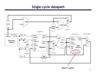
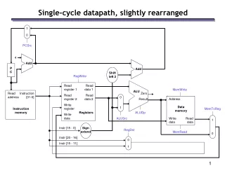
Single Cycle Datapath What are the performance limitations of this datapth?
Why Multi-Cycle? • Single cycle datapath • Design for the worst case • Need to make the cycle time = 8ns per cycle • Multi-cycle datapth • Design for each individual instruction class • For the above example: cycle time = 2ns • Lw=10ns (5 cycles), sw=8ns (4 cycles), R-format=8ns(4 cycles), beq=6ns (3 cycles)
Multi-Cycle Approach • Break up the instructions into steps, each step takes a clock cycle • Balance the amount of work to be done • Restrict each cycle to use only one major functional unit • At the end of a cycle • Store values for use in later cycles (easiest thing to do) • Introduce additional “internal” registers
Instruction Execution Steps Register-Register Instruction Fetch Instruction Decode Instruction ALU Operation Write Register Memory Read Instruction Fetch Instruction Decode Instruction Address Calculation Memory Read Write Register Memory Write Instruction Fetch Instruction Decode Instruction Branch Test & PC Update Branch Instruction Different instructions perform different operations at this step Fetch Instruction Decode Instruction Address Calculation Memory Write
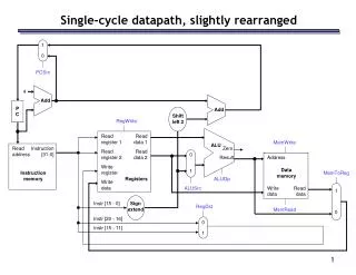
Multi-Cycle Datapath I o r D M e m R e a d M e m W r i t e I R W r i t e R e g D s t R e g W r i t e A L U S r c A P C 0 0 I n s t r u c t i o n R e a d M M [ 2 5 – 2 1 ] r e g i s t e r 1 A d d r e s s u u x R e a d x A I n s t r u c t i o n R e a d Z e r o d a t a 1 M e m o r y 1 1 [ 2 0 – 1 6 ] r e g i s t e r 2 A L U A L U A L U O u t 0 M e m D a t a R e g i s t e r s r e s u l t I n s t r u c t i o n W r i t e Fetch Instruction Decode Instruction Address Calculation Memory Read Write Register R e a d M B [ 1 5 – 0 ] r e g i s t e r d a t a 2 0 u I n s t r u c t i o n W r i t e x M [ 1 5 – 1 1 ] I n s t r u c t i o n 4 1 W r i t e d a t a 1 u r e g i s t e r d a t a 2 x 0 I n s t r u c t i o n 3 [ 1 5 – 0 ] M u x M e m o r y 1 1 6 3 2 d a t a A L U S h i f t S i g n r e g i s t e r c o n t r o l l e f t 2 e x t e n d I n s t r u c t i o n [ 5 – 0 ] M e m t o R e g A L U S r c B A L U O p New internal registers
Complete Control Lines What to write When to write P C W r i t e C o n d P C S o u r c e P C W r i t e A L U O p O u t p u t s I o r D A L U S r c B M e m R e a d A L U S r c A C o n t r o l M e m W r i t e R e g W r i t e M e m t o R e g O p R e g D s t I R W r i t e [ 5 – 0 ] 0 M 1 u J u m p 2 6 2 8 x I n s t r u c t i o n [ 2 5 – 0 ] a d d r e s s [ 3 1 - 0 ] S h i f t 2 l e f t 2 I n s t r u c t i o n [ 3 1 - 2 6 ] P C [ 3 1 - 2 8 ] P C 0 0 I n s t r u c t i o n R e a d M M [ 2 5 – 2 1 ] r e g i s t e r 1 u A d d r e s s u x x R e a d A I n s t r u c t i o n R e a d Z e r o M e m o r y 1 d a t a 1 1 [ 2 0 – 1 6 ] r e g i s t e r 2 A L U A L U A L U O u t 0 M e m D a t a R e g i s t e r s r e s u l t I n s t r u c t i o n W r i t e M R e a d B [ 1 5 – 0 ] r e g i s t e r u 0 I n s t r u c t i o n d a t a 2 W r i t e x [ 1 5 – 1 1 ] M I n s t r u c t i o n 4 1 W r i t e d a t a 1 u r e g i s t e r d a t a 2 x 0 I n s t r u c t i o n 3 [ 1 5 – 0 ] M u x M e m o r y 1 1 6 3 2 d a t a A L U S h i f t S i g n r e g i s t e r c o n t r o l l e f t 2 e x t e n d I n s t r u c t i o n [ 5 – 0 ]
Five Execution Steps • Instruction Fetch (IF) • Instruction Decode and Register Fetch (ID) • Execution, Memory Address Computation, or Branch Completion (EX) • Memory Access or R-type instruction completion (MEM) • Write-back step (WB)
Functional Behavior IF Instruction Fetch ID Instruction Decode Addr ALU Br J Instruction Execute MRd MWr Memory RWr RWr Register Writeback
Instruction Fetch Control IR = Memory[PC]; PC+=4 P C W r i t e C o n d P C S o u r c e P C W r i t e A L U O p O u t p u t s I o r D A L U S r c B M e m R e a d A L U S r c A C o n t r o l M e m W r i t e R e g W r i t e M e m t o R e g O p R e g D s t I R W r i t e [ 5 – 0 ] 0 M 1 u J u m p 2 6 2 8 x I n s t r u c t i o n [ 2 5 – 0 ] a d d r e s s [ 3 1 - 0 ] S h i f t 2 l e f t 2 I n s t r u c t i o n [ 3 1 - 2 6 ] P C [ 3 1 - 2 8 ] P C 0 0 I n s t r u c t i o n R e a d M M [ 2 5 – 2 1 ] r e g i s t e r 1 u A d d r e s s u x x R e a d A I n s t r u c t i o n R e a d Z e r o M e m o r y 1 d a t a 1 1 [ 2 0 – 1 6 ] r e g i s t e r 2 A L U A L U A L U O u t 0 M e m D a t a R e g i s t e r s r e s u l t I n s t r u c t i o n W r i t e M R e a d B [ 1 5 – 0 ] r e g i s t e r u 0 I n s t r u c t i o n d a t a 2 W r i t e x [ 1 5 – 1 1 ] M I n s t r u c t i o n 4 1 W r i t e d a t a 1 u r e g i s t e r d a t a 2 x 0 I n s t r u c t i o n 3 [ 1 5 – 0 ] M u x M e m o r y 1 1 6 3 2 d a t a A L U S h i f t S i g n r e g i s t e r c o n t r o l l e f t 2 e x t e n d I n s t r u c t i o n [ 5 – 0 ]
Instruction Fetch (IF) • Use PC to get instruction and put it in the Instruction Register. • Increment the PC by 4 and put the result back in the PC. • Can be described succinctly using RTL "Register-Transfer Language"IR = Memory[PC]; PC = PC + 4;Can we figure out the values of the control signals? • IR = Memory[PC];MemRead=1; IRWrite=1; IorD=0; • PC = PC + 4; ALUSrcA=0; ALUSrcB=01; ALUOp=00 (add); PCSource=00; PCWrite=1
P C W r i t e C o n d P C S o u r c e P C W r i t e A L U O p O u t p u t s I o r D A L U S r c B M e m R e a d A L U S r c A C o n t r o l M e m W r i t e R e g W r i t e M e m t o R e g O p R e g D s t I R W r i t e [ 5 – 0 ] 0 M 1 u J u m p 2 6 2 8 x I n s t r u c t i o n [ 2 5 – 0 ] a d d r e s s [ 3 1 - 0 ] S h i f t 2 l e f t 2 I n s t r u c t i o n [ 3 1 - 2 6 ] P C [ 3 1 - 2 8 ] P C 0 0 I n s t r u c t i o n R e a d M M [ 2 5 – 2 1 ] r e g i s t e r 1 u A d d r e s s u x x R e a d A I n s t r u c t i o n R e a d Z e r o M e m o r y 1 d a t a 1 1 [ 2 0 – 1 6 ] r e g i s t e r 2 A L U A L U A L U O u t 0 M e m D a t a R e g i s t e r s r e s u l t I n s t r u c t i o n W r i t e M R e a d B [ 1 5 – 0 ] r e g i s t e r u 0 I n s t r u c t i o n d a t a 2 W r i t e x [ 1 5 – 1 1 ] M I n s t r u c t i o n 4 1 W r i t e d a t a 1 u r e g i s t e r d a t a 2 x 0 I n s t r u c t i o n 3 [ 1 5 – 0 ] M u x M e m o r y 1 1 6 3 2 d a t a A L U S h i f t S i g n r e g i s t e r c o n t r o l l e f t 2 e x t e n d I n s t r u c t i o n [ 5 – 0 ] ID Stage: Assign A and B; Calculate Branch Address
Instruction Decode and Register Fetch (ID) • Still do not have any idea what instruction it is. • Read registers rs and rtin casewe need them • Compute the branch address (used in next cycle in casethe instruction is a branch) • RTL:A = Reg[IR[25-21]]; B = Reg[IR[20-16]];ALUOut = PC + (sign-extend(IR[15-0]) << 2); ALUSrcA = 0; ALUSrcB = 11; ALUOp = 00 (add); (for branch target)
P C W r i t e C o n d P C S o u r c e P C W r i t e A L U O p O u t p u t s I o r D A L U S r c B M e m R e a d A L U S r c A C o n t r o l M e m W r i t e R e g W r i t e M e m t o R e g O p R e g D s t I R W r i t e [ 5 – 0 ] 0 M 1 u J u m p 2 6 2 8 x I n s t r u c t i o n [ 2 5 – 0 ] a d d r e s s [ 3 1 - 0 ] S h i f t 2 l e f t 2 I n s t r u c t i o n [ 3 1 - 2 6 ] P C [ 3 1 - 2 8 ] P C 0 0 I n s t r u c t i o n R e a d M M [ 2 5 – 2 1 ] r e g i s t e r 1 u A d d r e s s u x x R e a d A I n s t r u c t i o n R e a d Z e r o M e m o r y 1 d a t a 1 1 [ 2 0 – 1 6 ] r e g i s t e r 2 A L U A L U A L U O u t 0 M e m D a t a R e g i s t e r s r e s u l t I n s t r u c t i o n W r i t e M R e a d B [ 1 5 – 0 ] r e g i s t e r u 0 I n s t r u c t i o n d a t a 2 W r i t e x [ 1 5 – 1 1 ] M I n s t r u c t i o n 4 1 W r i t e d a t a 1 u r e g i s t e r d a t a 2 x 0 I n s t r u c t i o n 3 [ 1 5 – 0 ] M u x M e m o r y 1 1 6 3 2 d a t a A L U S h i f t S i g n r e g i s t e r c o n t r o l l e f t 2 e x t e n d I n s t r u c t i o n [ 5 – 0 ] Execute: Memory TypeALUOut = A + offset (address)
P C W r i t e C o n d P C S o u r c e P C W r i t e A L U O p O u t p u t s I o r D A L U S r c B M e m R e a d A L U S r c A C o n t r o l M e m W r i t e R e g W r i t e M e m t o R e g O p R e g D s t I R W r i t e [ 5 – 0 ] 0 M 1 u J u m p 2 6 2 8 x I n s t r u c t i o n [ 2 5 – 0 ] a d d r e s s [ 3 1 - 0 ] S h i f t 2 l e f t 2 I n s t r u c t i o n [ 3 1 - 2 6 ] P C [ 3 1 - 2 8 ] P C 0 0 I n s t r u c t i o n R e a d M M [ 2 5 – 2 1 ] r e g i s t e r 1 u A d d r e s s u x x R e a d A I n s t r u c t i o n R e a d Z e r o M e m o r y 1 d a t a 1 1 [ 2 0 – 1 6 ] r e g i s t e r 2 A L U A L U A L U O u t 0 M e m D a t a R e g i s t e r s r e s u l t I n s t r u c t i o n W r i t e M R e a d B [ 1 5 – 0 ] r e g i s t e r u 0 I n s t r u c t i o n d a t a 2 W r i t e x [ 1 5 – 1 1 ] M I n s t r u c t i o n 4 1 W r i t e d a t a 1 u r e g i s t e r d a t a 2 x 0 I n s t r u c t i o n 3 [ 1 5 – 0 ] M u x M e m o r y 1 1 6 3 2 d a t a A L U S h i f t S i g n r e g i s t e r c o n t r o l l e f t 2 e x t e n d I n s t r u c t i o n [ 5 – 0 ] Execute: R- TypeALUOut = A op B
P C W r i t e C o n d P C S o u r c e P C W r i t e A L U O p O u t p u t s I o r D A L U S r c B M e m R e a d A L U S r c A C o n t r o l M e m W r i t e R e g W r i t e M e m t o R e g O p R e g D s t I R W r i t e [ 5 – 0 ] 0 M 1 u J u m p 2 6 2 8 x I n s t r u c t i o n [ 2 5 – 0 ] a d d r e s s [ 3 1 - 0 ] S h i f t 2 l e f t 2 I n s t r u c t i o n [ 3 1 - 2 6 ] P C [ 3 1 - 2 8 ] P C 0 0 I n s t r u c t i o n R e a d M M [ 2 5 – 2 1 ] r e g i s t e r 1 u A d d r e s s u x x R e a d A I n s t r u c t i o n R e a d Z e r o M e m o r y 1 d a t a 1 1 [ 2 0 – 1 6 ] r e g i s t e r 2 A L U A L U A L U O u t 0 M e m D a t a R e g i s t e r s r e s u l t I n s t r u c t i o n W r i t e M R e a d B [ 1 5 – 0 ] r e g i s t e r u 0 I n s t r u c t i o n d a t a 2 W r i t e x [ 1 5 – 1 1 ] M I n s t r u c t i o n 4 1 W r i t e d a t a 1 u r e g i s t e r d a t a 2 x 0 I n s t r u c t i o n 3 [ 1 5 – 0 ] M u x M e m o r y 1 1 6 3 2 d a t a A L U S h i f t S i g n r e g i s t e r c o n t r o l l e f t 2 e x t e n d I n s t r u c t i o n [ 5 – 0 ] Execute: Branch Typeif (A==B) PC=ALUOut
P C W r i t e C o n d P C S o u r c e P C W r i t e A L U O p O u t p u t s I o r D A L U S r c B M e m R e a d A L U S r c A C o n t r o l M e m W r i t e R e g W r i t e M e m t o R e g O p R e g D s t I R W r i t e [ 5 – 0 ] 0 M 1 u J u m p 2 6 2 8 x I n s t r u c t i o n [ 2 5 – 0 ] a d d r e s s [ 3 1 - 0 ] S h i f t 2 l e f t 2 I n s t r u c t i o n [ 3 1 - 2 6 ] P C [ 3 1 - 2 8 ] P C 0 0 I n s t r u c t i o n R e a d M M [ 2 5 – 2 1 ] r e g i s t e r 1 u A d d r e s s u x x R e a d A I n s t r u c t i o n R e a d Z e r o M e m o r y 1 d a t a 1 1 [ 2 0 – 1 6 ] r e g i s t e r 2 A L U A L U A L U O u t 0 M e m D a t a R e g i s t e r s r e s u l t I n s t r u c t i o n W r i t e M R e a d B [ 1 5 – 0 ] r e g i s t e r u 0 I n s t r u c t i o n d a t a 2 W r i t e x [ 1 5 – 1 1 ] M I n s t r u c t i o n 4 1 W r i t e d a t a 1 u r e g i s t e r d a t a 2 x 0 I n s t r u c t i o n 3 [ 1 5 – 0 ] M u x M e m o r y 1 1 6 3 2 d a t a A L U S h i f t S i g n r e g i s t e r c o n t r o l l e f t 2 e x t e n d I n s t r u c t i o n [ 5 – 0 ] Execute: Jump Type (New PC)
Execute, memory or branch (EX: instruction dependent) • The first cycle, the operation is determined by the instruction class • ALU is performing one of the following functions, based on instruction type • Memory Reference:ALUOut = A + sign-extend(IR[15-0]);ALUSrcA=1; ALUSrcB=10; ALUop=00 (add) • R-type:ALUOut = A op B;ALUSrcA=1; ALUSrcB=00; ALUop=10 (funct, inst[5:0], decides op) • Branch: if (A==B) PC = ALUOut; PCSource=01; ALUSrcA=1; ALUSrcB=00; ALUop=01 (sub); PCWriteCond=1; PCWrite=0; • Jump: PC = {PC[31:28] || IR[25:0] || 2‘b00}; PCSource=10; PCWrite=1;
P C W r i t e C o n d P C S o u r c e P C W r i t e A L U O p O u t p u t s I o r D A L U S r c B M e m R e a d A L U S r c A C o n t r o l M e m W r i t e R e g W r i t e M e m t o R e g O p R e g D s t I R W r i t e [ 5 – 0 ] 0 M 1 u J u m p 2 6 2 8 x I n s t r u c t i o n [ 2 5 – 0 ] a d d r e s s [ 3 1 - 0 ] S h i f t 2 l e f t 2 I n s t r u c t i o n [ 3 1 - 2 6 ] P C [ 3 1 - 2 8 ] P C 0 0 I n s t r u c t i o n R e a d M M [ 2 5 – 2 1 ] r e g i s t e r 1 u A d d r e s s u x x R e a d A I n s t r u c t i o n R e a d Z e r o M e m o r y 1 d a t a 1 1 [ 2 0 – 1 6 ] r e g i s t e r 2 A L U A L U A L U O u t 0 M e m D a t a R e g i s t e r s r e s u l t I n s t r u c t i o n W r i t e M R e a d B [ 1 5 – 0 ] r e g i s t e r u 0 I n s t r u c t i o n d a t a 2 W r i t e x [ 1 5 – 1 1 ] M I n s t r u c t i o n 4 1 W r i t e d a t a 1 u r e g i s t e r d a t a 2 x 0 I n s t r u c t i o n 3 [ 1 5 – 0 ] M u x M e m o r y 1 1 6 3 2 d a t a A L U S h i f t S i g n r e g i s t e r c o n t r o l l e f t 2 e x t e n d I n s t r u c t i o n [ 5 – 0 ] MEM: Load
Memory Access or R-Type • Loads and stores access memoryMDR = Memory[ALUOut];IorD=1; MemRead=1; or Memory[ALUOut] = B;IorD=1; MemWrite=1 • R-type instructions finishReg[IR[15-11]] = ALUOut;RegDst=1; MemtoReg=0; RegWrite =1
P C W r i t e C o n d P C S o u r c e P C W r i t e A L U O p O u t p u t s I o r D A L U S r c B M e m R e a d A L U S r c A C o n t r o l M e m W r i t e R e g W r i t e M e m t o R e g O p R e g D s t I R W r i t e [ 5 – 0 ] 0 M 1 u J u m p 2 6 2 8 x I n s t r u c t i o n [ 2 5 – 0 ] a d d r e s s [ 3 1 - 0 ] S h i f t 2 l e f t 2 I n s t r u c t i o n [ 3 1 - 2 6 ] P C [ 3 1 - 2 8 ] P C 0 0 I n s t r u c t i o n R e a d M M [ 2 5 – 2 1 ] r e g i s t e r 1 u A d d r e s s u x x R e a d A I n s t r u c t i o n R e a d Z e r o M e m o r y 1 d a t a 1 1 [ 2 0 – 1 6 ] r e g i s t e r 2 A L U A L U A L U O u t 0 M e m D a t a R e g i s t e r s r e s u l t I n s t r u c t i o n W r i t e M R e a d B [ 1 5 – 0 ] r e g i s t e r u 0 I n s t r u c t i o n d a t a 2 W r i t e x [ 1 5 – 1 1 ] M I n s t r u c t i o n 4 1 W r i t e d a t a 1 u r e g i s t e r d a t a 2 x 0 I n s t r u c t i o n 3 [ 1 5 – 0 ] M u x M e m o r y 1 1 6 3 2 d a t a A L U S h i f t S i g n r e g i s t e r c o n t r o l l e f t 2 e x t e n d I n s t r u c t i o n [ 5 – 0 ] MEM: Store
P C W r i t e C o n d P C S o u r c e P C W r i t e A L U O p O u t p u t s I o r D A L U S r c B M e m R e a d A L U S r c A C o n t r o l M e m W r i t e R e g W r i t e M e m t o R e g O p R e g D s t I R W r i t e [ 5 – 0 ] 0 M 1 u J u m p 2 6 2 8 x I n s t r u c t i o n [ 2 5 – 0 ] a d d r e s s [ 3 1 - 0 ] S h i f t 2 l e f t 2 I n s t r u c t i o n [ 3 1 - 2 6 ] P C [ 3 1 - 2 8 ] P C 0 0 I n s t r u c t i o n R e a d M M [ 2 5 – 2 1 ] r e g i s t e r 1 u A d d r e s s u x x R e a d A I n s t r u c t i o n R e a d Z e r o M e m o r y 1 d a t a 1 1 [ 2 0 – 1 6 ] r e g i s t e r 2 A L U A L U A L U O u t 0 M e m D a t a R e g i s t e r s r e s u l t I n s t r u c t i o n W r i t e M R e a d B [ 1 5 – 0 ] r e g i s t e r u 0 I n s t r u c t i o n d a t a 2 W r i t e x [ 1 5 – 1 1 ] M I n s t r u c t i o n 4 1 W r i t e d a t a 1 u r e g i s t e r d a t a 2 x 0 I n s t r u c t i o n 3 [ 1 5 – 0 ] M u x M e m o r y 1 1 6 3 2 d a t a A L U S h i f t S i g n r e g i s t e r c o n t r o l l e f t 2 e x t e n d I n s t r u c t i o n [ 5 – 0 ] R-Type Completion
P C W r i t e C o n d P C S o u r c e P C W r i t e A L U O p O u t p u t s I o r D A L U S r c B M e m R e a d A L U S r c A C o n t r o l M e m W r i t e R e g W r i t e M e m t o R e g O p R e g D s t I R W r i t e [ 5 – 0 ] 0 M 1 u J u m p 2 6 2 8 x I n s t r u c t i o n [ 2 5 – 0 ] a d d r e s s [ 3 1 - 0 ] S h i f t 2 l e f t 2 I n s t r u c t i o n [ 3 1 - 2 6 ] P C [ 3 1 - 2 8 ] P C 0 0 I n s t r u c t i o n R e a d M M [ 2 5 – 2 1 ] r e g i s t e r 1 u A d d r e s s u x x R e a d A I n s t r u c t i o n R e a d Z e r o M e m o r y 1 d a t a 1 1 [ 2 0 – 1 6 ] r e g i s t e r 2 A L U A L U A L U O u t 0 M e m D a t a R e g i s t e r s r e s u l t I n s t r u c t i o n W r i t e M R e a d B [ 1 5 – 0 ] r e g i s t e r u 0 I n s t r u c t i o n d a t a 2 W r i t e x [ 1 5 – 1 1 ] M I n s t r u c t i o n 4 1 W r i t e d a t a 1 u r e g i s t e r d a t a 2 x 0 I n s t r u c t i o n 3 [ 1 5 – 0 ] M u x M e m o r y 1 1 6 3 2 d a t a A L U S h i f t S i g n r e g i s t e r c o n t r o l l e f t 2 e x t e n d I n s t r u c t i o n [ 5 – 0 ] WB for Load
Write-back for load operation • Reg[IR[20-16]]= MDR;MemtoReg=1; RegWrite=1; RegDst=0; What about all the other instructions?
Summary Example:
Multi-Cycle Datapath • Programs take only as long as they need to • Variable timing per instruction • Pick a base cycle time • Re-use hardware • Avoid unnecessary duplication of hardware • Revisit control • Combinational vs. state machine design
Simple Questions • How many cycles will it take to execute this code? lw $t2, 0($t3) lw $t3, 4($t3) beq $t2, $t3, Label #assume not add $t5, $t2, $t3 sw $t5, 8($t3)Label: ... • What is going on during the 8th cycle of execution? • In what cycle does the actual addition of $t2 and $t3 takes place? Example:
Implementing the Control (D.3) • Value of control signals is dependent upon: • What instruction is being executed • Which step is being performed • Use the information we have accumulated to specify a finite state machine • Specify the finite state machine graphically, or • Use microprogramming • Implementation can be derived from specification
Graphical Specification of FSM I n s t r u c t i o n d e c o d e / 0 I n s t r u c t i o n f e t c h 1 r e g i s t e r f e t c h M e m R e a d A L U S r c A = 0 I o r D = 0 A L U S r c A = 0 I R W r i t e A L U S r c B = 1 1 S t a r t A L U S r c B = 0 1 A L U O p = 0 0 A L U O p = 0 0 P C W r i t e P C S o u r c e = 0 0 ) ) ' e Q p ) y t ' E - J R B ' = ' p = = O ( ) ' p p W M e m o r y a d d r e s s S O ' B r a n c h O = J u m p ( p O ( c o m p u t a t i o n ( r o E x e c u t i o n c o m p l e t i o n ) c o m p l e t i o n ' W 2 6 8 9 L ' = p O ( A L U S r c A = 1 A L U S r c A = 1 A L U S r c B = 0 0 A L U S r c A = 1 P C W r i t e A L U S r c B = 1 0 A L U O p = 0 1 A L U S r c B = 0 0 P C S o u r c e = 1 0 A L U O p = 0 0 P C W r i t e C o n d A L U O p = 1 0 P C S o u r c e = 0 1 ( O ) p ' = W ' S L ' W ' = ) p M e m o r y M e m o r y O ( a c c e s s a c c e s s R - t y p e c o m p l e t i o n 3 5 7 R e g D s t = 1 M e m R e a d M e m W r i t e R e g W r i t e I o r D = 1 I o r D = 1 M e m t o R e g = 0 4 W r i t e - b a c k s t e p R e g D s t = 0 R e g W r i t e M e m t o R e g = 1
Finite State Machine for Control P C W r i t e P C W r i t e C o n d I o r D M e m R e a d Control Logic M e m W r i t e I R W r i t e Alternatives for implementing the control logic? M e m t o R e g P C S o u r c e A L U O p Outputs A L U S r c B A L U S r c A R e g W r i t e R e g D s t N S 3 N S 2 Inputs N S 1 N S 0 4 3 2 1 0 5 p p p p p p 3 2 1 0 O O O O O O S S S S I n s t r u c t i o n r e g i s t e r S t a t e r e g i s t e r o p c o d e f i e l d
O p 5 O p 4 O p 3 O p 2 O p 1 O p 0 S 3 S 2 S 1 S 0 P C W r i t e P C W r i t e C o n d I o r D M e m R e a d M e m W r i t e I R W r i t e M e m t o R e g P C S o u r c e 1 P C S o u r c e 0 A L U O p 1 A L U O p 0 A L U S r c B 1 A L U S r c B 0 A L U S r c A R e g W r i t e R e g D s t N S 3 N S 2 N S 1 N S 0 PLA Implementation control signal and next state truth tables
ROM Implementation P C W r i t e • Very inefficient implementation • Mostly redundant entries • Dominated by next state function • Adding pipelined of FP instructions P C W r i t e C o n d I o r D M e m R e a d 210x20 bit ROM M e m W r i t e I R W r i t e M e m t o R e g P C S o u r c e A L U O p Outputs A L U S r c B A L U S r c A R e g W r i t e R e g D s t N S 3 N S 2 Inputs N S 1 N S 0 4 3 2 1 0 5 p p p p p p 3 2 1 0 O O O O O O S S S S I n s t r u c t i o n r e g i s t e r S t a t e r e g i s t e r o p c o d e f i e l d
Sequencer Implementation (D.4) • Sequence through the state machine • What are my options? • Control branches in the state machine via dispatch tables
Control Flow Sequencing Options I n s t r u c t i o n d e c o d e / I n s t r u c t i o n f e t c h r e g i s t e r f e t c h M e m R e a d A L U S r c A = 0 I o r D = 0 A L U S r c A = 0 I R W r i t e A L U S r c B = 1 1 A L U S r c B = 0 1 A L U O p = 0 0 A L U O p = 0 0 P C W r i t e P C S o u r c e = 0 0 R = p O ( ) ' W M e m o r y a d d r e s s S ' B r a n c h = J u m p p O c o m p u t a t i o n ( r o E x e c u t i o n c o m p l e t i o n ) c o m p l e t i o n ' W L ' = p O ( A L U S r c A = 1 A L U S r c A = 1 A L U S r c B = 0 0 A L U S r c A = 1 P C W r i t e A L U S r c B = 1 0 A L U O p = 0 1 A L U S r c B = 0 0 P C S o u r c e = 1 0 A L U O p = 0 0 P C W r i t e C o n d A L U O p = 1 0 P C S o u r c e = 0 1 M e m o r y M e m o r y a c c e s s a c c e s s R - t y p e c o m p l e t i o n R e g D s t = 1 M e m R e a d M e m W r i t e R e g W r i t e I o r D = 1 I o r D = 1 M e m t o R e g = 0 W r i t e - b a c k s t e p R e g D s t = 0 R e g W r i t e M e m t o R e g = 1
Final Contents of Control ROM Separation of control flow and data
Specifying Control • Specifying all of the control bits for each state is tedious and error prone • Use a symbolic language • Each state is a microinstruction • Organize the control bits into fields microinstruction • Microprograms, microcode, and micropgramming ALU Control SRC Control REG Control MEM Control PC Control Sequencing
Exceptions • Distinguish between internal and external events that cause an unexpected change in flow of control • Exceptions vs. interrupts • I/O, service, OS traps, errors • Updates to the data path • Recording the cause of the exception and transferring control to the OS • Consider the impact of hardware modifications on the critical path
Exception Handling: Control • Record the cause of the exception • MIPS uses the a status register referred to as the cause register • Record the return address in the exception program counter (EPC) • Of the offending instruction or the following instruction • Transfer control • To a fixed address exception handler decodes the cause • Vectored exceptions target address encodes the cause
Exception Handling: Operations • Add two registers to the datapath • EPC and Cause registers • Add a state for each exception condition • Use the ALU to compute the EPC contents • Write the Cause register with exception condition • Update the PC with OS handler address • Generate control signals for each operation • See Appendix B.7 for details of MIPS 2000/3000 implementation
The OS Interactions • The MIPS 32 Status and Cause Registers 31 15 8 4 1 0 Status Register Interrupt Mask int enable User mode Excep level 31 15 8 6 2 0 Cause Register Branch Delay Pending Interrupts Exception Code • Operating System handlers interrogate these registers • Manage all state saving requirements • Read example in B.7
s t r u c t i o n d e c o d e / r e g i s t e r f e t c h R = p O ( ) ' W M e m o r y a d d r e s s S ' B r a n c h = J u m p p O c o m p u t a t i o n ( r o E x e c u t i o n c o m p l e t i o n ) c o m p l e t i o n ' W L ' = p O ( A L U S r c A = 1 A L U S r c A = 1 A L U S r c B = 0 0 A L U S r c A = 1 P C W r i t e A L A L U O p = 0 1 A L U S r c B = 0 0 P C S o u r c e = 1 0 P C W r i t e C o n d A L U O p = 1 0 P C S o u r c e = 0 1 M e m o r y M e m o r y a c c e s s a c c e s s R - t y p e c o m p l e t i o n R e g D s t = 1 M e m R e a d M e m W r i t e R e g W r i t e I o r D = 1 I o r D = 1 M e m t o R e g = 0 W r i t e - b a c k s t e p Exception Handling: State Machine I n I n s t r u c t i o n f e t c h 0 M e m R e a d 1 A L U S r c A = 0 I o r D = 0 A L U S r c A = 0 I R W r i t e A L U S r c B = 1 1 S t a r t A L U S r c B = 0 1 A L U O p = 0 0 A L U O p = 0 0 P C W r i t e P C S o u r c e = 0 0 ) ) ' e Q p ) y t ' E - J B ' ' = = p p O O ( ( 2 6 8 9 U S r c B = 1 0 A L U O p = 0 0 ( O ) p ' = W ' IllegalInstruction S L ' W ' = ) p Overflow O ( Intcause = 0 CauseWrite ALUSrcA = 0 ALUSrcB = 01 ALUOp = 01 EPCWrite PCWrite PCSource = 11 Intcause = 1 CauseWrite ALUSrcA = 0 ALUSrcB = 01 ALUOp = 01 EPCWrite PCWrite PCSource = 11 3 5 7 4 R e g D s t = 0 R e g W r i t e M e m t o R e g = 1
Exception Handling: Datapath IntCause EPCWrite Causewrite P C W r i t e C o n d P C S o u r c e P C W r i t e A L U O p O u t p u t s I o r D A L U S r c B M e m R e a d A L U S r c A C o n t r o l M e m W r i t e R e g W r i t e M e m t o R e g O p R e g D s t I R W r i t e [ 5 – 0 ] 0 M 1 u J u m p 2 6 2 8 x I n s t r u c t i o n [ 2 5 – 0 ] a d d r e s s [ 3 1 - 0 ] S h i f t 2 l e f t 2 I n s t r u c t i o n 0x80000180 3 [ 3 1 - 2 6 ] P C [ 3 1 - 2 8 ] P C 0 0 I n s t r u c t i o n R e a d M M [ 2 5 – 2 1 ] r e g i s t e r 1 u A d d r e s s u x x R e a d A I n s t r u c t i o n R e a d Z e r o M e m o r y 1 d a t a 1 1 [ 2 0 – 1 6 ] r e g i s t e r 2 A L U A L U A L U O u t 0 M e m D a t a R e g i s t e r s r e s u l t I n s t r u c t i o n W r i t e M R e a d B [ 1 5 – 0 ] r e g i s t e r u 0 I n s t r u c t i o n d a t a 2 W r i t e x [ 1 5 – 1 1 ] M EPC I n s t r u c t i o n 4 1 W r i t e d a t a 1 u r e g i s t e r d a t a 2 x 0 I n s t r u c t i o n 3 [ 1 5 – 0 ] M u x 0 0 M e m o r y 1 M 1 6 3 2 d a t a A L U u Cause S h i f t S i g n r e g i s t e r c o n t r o l x l e f t 2 e x t e n d 1 1 I n s t r u c t i o n [ 5 – 0 ]
Study Guide • Given a MIPS 32 instruction sequence • Reproduce the sequence of states generated by the controller • Compute the execution time in cycles • Determine all control signal values if the system is frozen at an arbitrary clock cycle • Modify the datapath and state machine to • Add new exception conditions • New instructions • Extend the memory system where an access takes 2 cycles instead of 1 cycle • Modify microcode to add instructions • Draw the multicycle datapath from memory
Glossary • Dispatch table • Exception • Finite State Machine • Instruction decode • Instruction fetch • Microinstruction • Microprogramming • Microcode • Multi-Cycle datapath • Sequencer • ROM