Download
1 / 61
610 likes | 704 Views
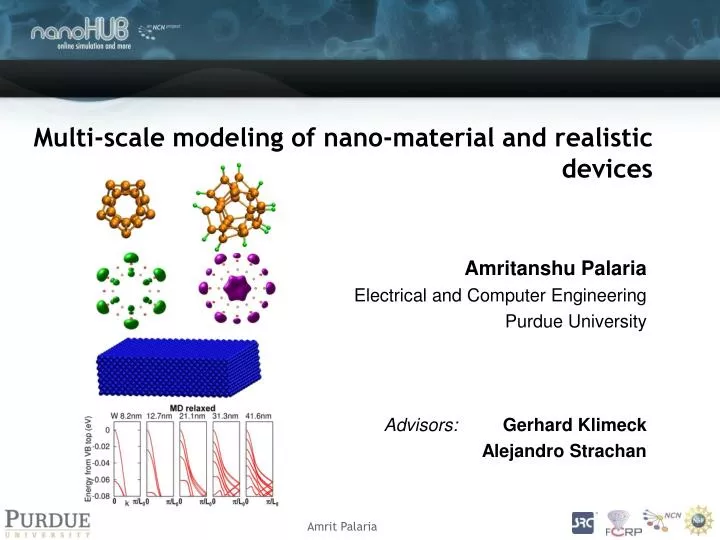
Multi-scale modeling of nano-material and realistic devices. Amritanshu Palaria Electrical and Computer Engineering Purdue University Advisors: Gerhard Klimeck Alejandro Strachan. Si nanowire array FET (Wang et al., 2006). Si nanowire inverter (Cui and Leiber, 2000).

E N D
Multi-scale modeling of nano-material and realistic devices Amritanshu Palaria Electrical and Computer Engineering Purdue University Advisors: Gerhard Klimeck Alejandro Strachan
Si nanowire array FET (Wang et al., 2006) Si nanowire inverter (Cui and Leiber, 2000) Introduction Why material modeling? Challenges in continuing Moore’s law: transistors, interconnects Desired device properties new material new device/ architecture ITRS 2007 - 1D nanostructure extensions to CMOS ITRS 2007
Introduction Why material modeling? • Nanowires - New materials! • Properties tunable by size. • • Electrical and optical properties • Can be the most confining electrical conductors - squeeze electrons • Can be defect free • Quantum confinement - tunable optical properties • • Mechanical properties • Can exhibit high strengths • • Thermal properties • - Can be designed to conduct heat much better or worse than bulk • • Chemical properties • - Dominated by large surface-to-volume ratio
Introduction Why material modeling? Chen and Carlen, Univ of Twente Other applications of silicon nanowires: • Chemical sensors (large surface) • Energy conversion devices • Thermoelectric devices • Photovoltaic • Electrochemical storage (lithium battery electrode) Garnett and Yang, 2008 ZT = S2σT/κ Peng et al., 2005 p n n p Chan et al., 2008
3D - diamond (sp3) Insulating 3D - graphite (sp2) 2D - graphene 1D - carbon nanotubes (picture by Jannik Meyer) (TEAM 0.5, Berkeley Lab) 0D - buckminster fullerene Anisotropically conducting Superconducting Semiconducting/ metallic Insulating (fullerite) Introduction Why material modeling? Material details drastically affect electrical properties Dimensionality and bonding affect electrical properties Example of Carbon
Introduction Multi-scale modeling Electrical Engineering Material Science Size of System Size of System Continuum Semi-classical (BTE) Classical Molecular dynamics Mesoparticle Quantum Mechanics (DFT/ GW) Quantum (NEGF) Resolution Resolution BULK BULK NANOTUBES SUB-MICRON MOSFET NANOTUBES COLLOIDS GRAINS Resolution Generality/ transferability At atomistic level the paths converge
Introduction Multi-scale modeling Size of System Size of System Continuum 1. Atomic Structure Semi-classical (BTE) Classical Molecular dynamics Eg, m* Mesoparticle Quantum Mechanics (DFT/ GW) Quantum (NEGF) Resolution Resolution 2. Tight-binding Model
Channel Molecular structure Channel Hamiltonian MD/ DFT Tight Binding Introduction Multi-scale modeling - Vision Structural Quantum Mechanics Electrostatics Poisson Statistical Mechanics Boltzmann/ NEGF <1nm diameter SiNW strained Si/Ge/Si nanobars TB for surfaces
Geometry morphology and properties of 1 nm silicon nanowires Amrit Palaria, Alejandro Strachan, Gerhard Klimeck Objective: Investigate stability and properties of ~1nm diameter 1-D silicon nano-structures Method:Multi-scale modeling in time - density functional theory, reactive force field molecular dynamics • Results: • 2 categories of energetically most stable Si nanowires (NW) of dia ~ 1nm • Stable wires possess non-diamond geometries • Structural symmetry reduction at wire surface enhances stability and introduces bandgap • Pristine and H passivated wires with new bandgaps and unique properties • Impact: • New materials: possible use in thermoelectrics, photovoltaics, sensors, flexible electronics, CMOS scaling • General method for exploration of new materials
Electronic properties of Si-Ge-Si heterostructures from tight binding Amrit Palaria, Gerhard Klimeck, Alejandro Strachan Objective:Investigate the electronic bandstructure properties of s-Si/s-Ge/s-Si nanowires with major Ge section • Method: • Use realisitc Si-Ge-Si nanowire structures obtained from ReaxFF molecular dynamics • Model the Ge section of the wires using bulk sp3d5s* tight binding parameters modified for strain • Results: • Hole effective mass of wire structured from 2% compressively strained Ge film reduces with decreasing width • General VB shape is dependent on average strain • Non-uniformity of strain plays a role in effective mass and DOS • Impact: • Can provide channel material for faster devices (high gm)
Tight binding parameters for silicon surface Amrit Palaria, Gerhard Klimeck, Alejandro Strachan Objective:Investigate the possibility of simulating surfaces and interfaces with empirical tight binding • Method: • Investigate sp3d5s* tight binding using bulk with strain parameters for Si slab with (100) surface, modify NEMO-3D for this (in C++) • Use GW results as benchmark • Modify surface atom bulk parameters • Check sensitivity of high symmetry points to bulk parameter modification • Impact: • Quick and scalable simulation of realistic electronic devices with surfaces or other non-bulk bonds e.g. interfaces • Result: • Band-structure of Si(100) surface from TB with modified sigma parameters matches reasonably with GW results
Structures and properties of very small diameter (<1 nm) Si nanowires
Introduction Why material modeling? • Nanowires - New materials! • Properties tunable by size. • • Electrical and optical properties • Can be the most confining electrical conductors - squeeze electrons • Can be defect free • Quantum confinement - tunable optical properties • • Mechanical properties • Can exhibit high strengths • • Thermal properties • - Can be designed to conduct heat much better or worse than bulk • • Chemical properties • - Dominated by large surface-to-volume ratio
Introduction Why material modeling? Chen and Carlen, Univ of Twente Other applications of silicon nanowires: • Chemical sensors (large surface) • Energy conversion devices • Thermoelectric devices • Photovoltaic • Electrochemical storage (lithium battery electrode) Garnett and Yang, 2008 ZT = S2σT/κ Peng et al., 2005 p n n p Chan et al., 2008
Introduction Why worry about such small diameters? Bandgap increases with decreasing diameter dia (nm) Source: American Society for Testing and Materials (ASTM) Thermoelectric performance can improve with decreasing diameter ZT = PT/(κe+κph) Wire Liang and Li, 2006 Shi et al, 2009
SiNW with dia <2 nm achieved! (Ma et al., Science, 2003) Hydrogen passivated surface Claim - silicon bulk configuration Background of small diameter silicon nanowires Silicon nanowires with bulk geometry • Few nm diameter - bulk geometry (Wu et al., Nano Lett., 2005) ~4nm diameter No surface oxide [110] wire preferred
Background of small diameter silicon nanowires Non-bulk geometry wires - role of surfaces • ~1 nm unpassivated wires? (DFT study, Kagimura et al., PRL, 2005) [110] Simple hexagonal • Non CNT structure silicon nanotubes (Bai et al., PNAS 2003) DFT-GGA <1nm diameter Hexagonal, pentagonal, square cross sections Metastable Metallic
Introduction Objectives • What are the energetically most stable 1-D silicon nanostructures at ~1nm diameter – unpassivated and H-passivated? • What are some electronic properties of these structures? • Can we understand the physics of the surface effect on the stability and properties of these structures?
Introduction Objectives • What are the energetically most stable 1-D silicon nanostructures at ~1nm diameter – unpassivated and H-passivated? • What are some electronic properties of these nanowires? • Can we understand the physics of the surface effect on the stability and properties of these structures?
Force-field Molecular Dynamics FF-MD Predicting new material Predicting Si nanowire structure Energy Eb barrier height generalized coordinate ReaxFF-MD (fast and inexpensive) exploration tool Density Functional Theory DFT SeqQuest/ Abinit (expensive) refinement tool fs ps ns Simulated Time
Predicting new material Using reactive force field MD as exploratory tool Example with compression speed 5A/ns Expansion Compression
(eV/atom) 0.635 Predicting new material ~1 nm dia silicon nanowires 0.637 Energetically most stable unpassivated wires: tubular 2 categories: Distorted fullerenes (DF) Distorted nanotubes (DNT) Surface modifies geometry Very different from diamond bulk or carbon nanotubes! 0.638 0.658 0.673 sp3 sp2 0.697 0.705 0.708 0.714 (eV/atom)
(eV/atom) {(E|t),D5h} 0.635 Predicting new material ~1 nm dia silicon nanotubes {(E|t),D1h} 0.637 {(E|t),D6h} 0.638 Low symmetry High disorder {(E|t),(v|t/2)} 0.658 {(E|t), C1v} 0.673 0.697 {(E|t),(C12|t/2),D6h} 0.705 0.708 {(E|t),(C10|t/2),D5h} 0.714 (eV/atom)
Predicting new material ~1 nm dia H passivated silicon nanowires DF1 Energy DNTs and Fs better than or comparable to diamond wires + H : Esur Esur:H H F1
Introduction Objectives • What are the energetically most stable 1-D silicon nanostructures at ~1nm diameter – unpassivated and H-passivated? • 2 categories of tubular non diamond-core silicon nanowires: • DFs and DNTs • What are some electronic properties of these structures? • Can we understand the physics of the surface effect on the stability and properties of these structures?
110_small F1 DNT3 F2 DNT1 Properties of Si nanotubes Effective masses of ~1 dia silicon nanowires DF1 DNT3 DNT1 DF2’ Unpassivated /ɑF1 /ɑDNT1 /ɑF2 /ɑDNT3 /ɑ[110] 0 0 0 0 0 0 bandgap H-passivated
Properties of Si nanotubes Kohn-Sham bandgaps: the bandgap problem Non-interacting system Actual interacting system Same ρ(r) Kohn-Sham DFT is not designed to determine correct single particle states
Properties of Si nanotubes Kohn-Sham bandgaps: the bandgap problem • DFT not designed to determine correct single particle states. • Yet known to provide: • almost correct dispersion for filled states in ground state system • almost correct curvatures of single particle states • smaller than true bandgap • prediction of presence of gap from DFT is correct • for SiNW, the GW bandgap is proportional to K-S bandgap(Zhao et al., 2004)
Properties of Si nanotubes Electronic band gaps of bulk like silicon nanowires For silicon (bulk, surface, bulk-like nanowires): BandgapGW ~ 2*BandgapK-S (sp3d5s* TB)
Properties of Si nanotubes Electronic band gaps of ~1 dia silicon nanowires New bandgaps Diamond wires (DFT) DFT Visible (guess)
110_small F1 DNT3 F2 DNT1 Properties of Si nanotubes Effective masses of ~1 dia silicon nanowires DF1 DNT3 DNT1 DF2’ Unpassivated /ɑF1 /ɑDNT1 /ɑF2 /ɑDNT3 /ɑ[110] 0 0 0 0 0 Non-diamond wires have high effective masses H-passivated
Properties of Si nanotubes Investigating mechanical response 118 Young’s moduli (GPa) 72 145 Not too different from bulk (80 GPa for Si bulk) Good strength => Flexible electronics: Straining F1 using ReaxFF MD at 300K Sustains 6% strain Bulk can sustain only 0.04%
Introduction Objectives • What are the energetically most stable 1-D silicon nanostructures at ~1nm diameter – unpassivated and H-passivated? • 2 categories of tubular non diamond-core silicon nanowires: • DFs and DNTs • What are some electronic properties of these structures? • New bandgaps and effective masses • Can we understand the physics of the surface effect on the stability and properties of these structures?
Properties of Si nanotubes What leads to higher gap in lower energy structures? Unpassivated wires
x y z bohr-3/2 bohr-3/2 Properties of Si nanotubes What leads to gap in lower energy structures? Symmetry of structure same symmetry of HOMO and LUMO bohr-3/2 bohr-3/2 Loss of structure symmetry loss of similarity in symmetries of HOMO and LUMO
A’ A F1 and DF1 Si (100) p(2X1) surface reconstruction Properties of Si nanotubes Comparison with Si (100) surface Perfect fullerene Distorted fullerene - DF1 F1 DF1 + A’ A F1 Asymmetric A A’ Symmetric Symmetry breaking of structure redistributes HOMO e- among atoms Similar to Si(100) symmetric to asymmetric reconstruction
Introduction Objectives • What are the energetically most stable 1-D silicon nanostructures at ~1nm diameter – unpassivated and H-passivated? • 2 categories of tubular non diamond-core silicon nanowires: • DFs and DNTs • What are some electronic properties of these structures? • New bandgaps and effective masses • Can we understand the physics of surface effect on the stability and properties of these structures? • Loss of structural symmetry leads to enhanced stability and redistribution of HOMO electrons among atoms leading to a bandgap
Strained Si/Ge/Si hetero nanobars The structure Periodic
Strained Si/Ge/Si hetero nanobars Objectives • What are the confinement effects on electronic bandstructure? • What are the strain effects? How does MD relaxed differ from homogeneous uniaxially or biaxially strained wire? Are the properties of MD relaxed wires good or bad for devices? • Does non-uniformity of strain play any role?
Transverse strain vs W and H Strained Si/Ge/Si hetero nanobars Introduction Virtual SiGe W Hashemi et al., 2007 H SiO2 2% -2% 2% 2% 2% -2% -2% Si -2% -2% 2% 2% 2% W: 30-300nm Si Transverse Transverse Ge Longitudinal Longitudinal Ge Si Si Strain relaxes SiO2 Virtual SiGe Hashemi et al., 2007 Park et al., JAP, 2009 H = 6.39 nm, W = 20.09 nm ReaxFF MD W Square Ge sections - almost uniaxial strain
Strained Si/Ge/Si hetero nanobars Structures and Method Periodic EV > 0.4eV p-type device H ~ 7 nm H ~ 10 nm W: 8-41 nm sp3d5s* tight binding with strain corrections (Boykin et al., 2002) and surface passivation (Lee et al., 2004)
Strained Si/Ge/Si hetero nanobars Strains Longitudinal (periodic) W~8nm H W~12nm H~7nm W W~30nm
Strained Si/Ge/Si hetero nanobars Strains Asterisks: peaks of distribution Green dotted line: average transverse strain Variation of bond strains in MD relaxed wires Compared with uniformly uniaxial and uniformly biaxial wires with 2% compression in longitudinal direction
Strained Si/Ge/Si hetero nanobars Confinement effect VB edge CB edge Band edges Effective masses Bulk: (/ɑ, /ɑ, 0) to (/ɑ, /ɑ, /ɑ) Slab: (/ɑ, /ɑ, 0) to (/ɑ, /ɑ, /ɑ) Wire: (0, 0, 0) to (0, 0, /ɑ) Bulk: (0, 0, 0) to (0, 0, /ɑ) Slab: (0, 0, 0) to (0, 0, /ɑ) Wire: (0, 0, 0) to (0, 0, /ɑ) • bulkslabwire: • Bandgaps increase • Effective masses degrade
Strained Si/Ge/Si hetero nanobars Ge wires VB CB • Shifts in band edges • Changes in band curvatures
Strained Si/Ge/Si hetero nanobars Band edges in Ge wires Filled symbols: H~7nm Open symbols: H~10nm • Bandgaps increase with decreasing widths • MD relaxed has smallest bandgap (smaller by about 0.1eV than uniaxial wire)
Strained Si/Ge/Si hetero nanobars Electron effective masses in Ge wires Filled symbols: H~7nm Open symbols: H~10nm • Branches switch at band edge, causing the effective masses to oscillate with changing widths. • MD relaxed has close to or higher effective mass than uniaxial.
Strained Si/Ge/Si hetero nanobars Hole effective masses in Ge wires Filled symbols: H~7nm Open symbols: H~10nm • MD relaxed band edge effective mass remains close to uniaxial. • Average effective mass is smaller than even uniaxial for smalle widths and increases with increasing width!
Strained Si/Ge/Si hetero nanobars Valence bands of MD relaxed wires Degradation in effective mass appears to come from faster curving of valence bands to become concave up