Download
1 / 9
100 likes | 219 Views
EEE324 Digital Electronics. Lecture 3: Circuits. Ian McCrum Room 5B18, 02890366364 IJ.McCrum@ulster.ac.uk http://www.eej.ulst.ac.uk/~ian/modules/EEE342. Simple Digital Logic.

E N D
EEE324 Digital Electronics Lecture 3:Circuits Ian McCrum Room 5B18, 02890366364 IJ.McCrum@ulster.ac.uk http://www.eej.ulst.ac.uk/~ian/modules/EEE342
Simple Digital Logic • There is a free software tool from the Altera corporation that allows experimenting with logic circuitry – to manipulate ‘1’s and ‘0’s • The package is called Quartus – it is a large download. • Designed to convert schematic or hardware descriptions into circuits that can be “downloaded” into special chips it also has a useful circuit simulator. • Go to WWW.ALTERA.COM and download the free web edition of Quartus.
Digital circuits • To create a design you can use a text editor or a schematic drawing tool. It is easier to begin with the scematic tool. • When we design larger circuits we can use a text language and use software to convert this to functional blocks and interconnections • Here we will use single bits to get the concepts across.
Digital circuits NOT gate AND gate OR gate EX-OR gate NAND gate NOR gate EX-NOR gate MUX (2 to 1) MUX (4 to 1) Taken from http://www.rapidtables.com/electric/electrical_symbols.htm
A D Truth Tables F F B The NOT gate, also called an INVERTOR A ‘1’ in produces a ‘0’ out A ‘0’ in produces a ‘1’ out The input is on the left and the output on the right C The AND gate A B || F 0 0 || 0 0 1 || 0 10 || 0 1 1 || 1 The OR gate CD || F 0 0 || 0 0 1 || 1 1 0 || 1 1 1 || 1 We can consider these as functions of boolean logic, there is an extensive algebra to work with. For CPU design we only need a few gates, they tend to function as gates rather than functional blocks. Note how we can interpret the truth tables if we consider one input to be carrying DATA and the other to be controlling the flow of that DATA through the gate. E.g if A is HIGH in the AND gate then the output is the input. If A is LOW the output is forced low. We can use AND gates to selectively reset signals E.g if C is LOW in the OR gate then the output is the input. If C is HIGH the output is forced HIGH. We can use OR gates to selectively set signals (We can use EX-OR gates to invert or not invert signals)
Muxes (Multiplexors) An extremely useful component in computer design If S0 is LOW then the output F is the same as the input A if S0 is HIGH then the output F is the same as the input B We can draw a truth table for this device but it is easier to learn the sentences above. A F B S0 Generate a ‘1’ when the input is 010 or 011 or 101 or 111. F(S0,A,B) = /S0.A./B + /S0.A.B + S0./A.B + S0.A.B This is known as the AND-OR equation representing the truth table on the left. (aka Sum of Products form) Each AND gate decodes a PRODUCT TERM. Truth table for 2 to 1 multiplexor S0 A B || F 0 0 0 || 0 0 0 1 || 0 01 0 || 1 01 1 || 1 1 0 0 || 0 1 0 1 || 1 1 1 0 || 0 1 1 1 || 1 It is simply a switch to route data
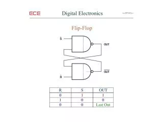
One Bit Stores • By using feedback internally we can create a block that can remember a value. These are usually called flipflops and come in various types. Here we need only consider the D-type • A D-type flipflop has one data input labelled D and a further input labelled CLOCK. The output is usually labelled Q and is complemented with a further output of NOT-Q. For simple computer circuit we can ignore NOT-Q. • The CLOCK is usually connected to a regular square wave running at a fixed frequency. Or to a control signal from another part of our circuit. There are limits as to how fast the CLOCK can be. Truth tables are inadequate to describe memory, we can use a variant called a characteristic table. But just think of the device “capturing” the input at the instant of a rising edge on the clock signal
Registers 8 8 Imagine 8 D-types With all the CLOCK Inputs connected together. And the 8 D inputs considered As carrying an 8 bit Binary number. We have created a “REGISTER” which can capture an 8 bit number and hold it Until it gets overwritten with a new value. CLK
Summary • Know the basic gates – NOT, AND, OR • Know the operation of a MUX • Know the operation of a D-type • Know how an 8 bit register works. • You are now ready to design complete CPUs!