Download
1 / 59
670 likes | 849 Views
Digital Electronics. Module 3 Combinational and Sequential Logic Circuits [4 weeks]. Objectives. 1.Describe the operation of the XOR, XNOR gates ...[week-1] 2. Describe the operation of the clocked and un-clocked SR-Latch.... [week-2]

E N D
Digital Electronics Module 3Combinational and Sequential Logic Circuits [4 weeks]
Objectives 1.Describe the operation of the XOR, XNOR gates...[week-1] 2. Describe the operation of the clocked and un-clockedSR-Latch....[week-2] 3.Describe the operation of the D and JK Flip Flops....[week-3] 4.Distinguish between combinational logic and sequential logic. ...[week-4 ] 5.Use of sequential logic in simpleapplications. • ….[week-4]
INTRODUCTION • What is combinational logic? • What are the combinational logic gates? • What are the applications? • Answer is very simple Go to Google and search
Combinational logic: • When logic gates (such as AND, OR and NOT) are connected together to produce a specified output for certain specified combinations of input variables, with no storage involved, the resulting network is called combinational logic
Definition • The combinational logic can be defined as “is that logic in which all outputs are directly related to the current combination of values on its inputs”.
Combinational logic • Simple and often-used combinational logic circuits are XOR and XNOR. These two gates are actually formed by a combination of other gates .
http://www.youtube.com/watch?v=UCbhu5zaqqY • http://www.youtube.com/watch?NR=1&v=KaoT9wyJXic&feature=endscreen
The XOR Logic Circuit and Symbol http://tams-www.informatik.uni-hamburg.de/applets/hades/webdemos/10-gates/00-gates/xor.html
Referring to logic circuit in Figure 1, you can see how an XOR gate is made up of the combination of AND, OR, and NOT gates. • The standard symbol for the XOR gate is shown in Figure 2. • Note that XOR gate has only two inputs, it never has more than two inputs.
The logical operation of XOR is such that the output is high only when the two inputs are at opposite levels. • The operation of XOR with two inputs A and B and output X is stated as follows: • If A is LOW and B is HIGH, ORif A is HIGH and B is LOW, then X is HIGH • IfA and B are both HIGH or both LOW, then X isLOW X is HIGH when A&B are different.
XOR Logical Function • The two variables expression “X = AB” is called the Logical XOR Function. Referring to logic circuit in Figure 1, XOR function can be illustrated as follows:
The Exclusive-NOR (XNOR) • Referring to logic circuit in Figure ; you can see how an XNORgate is made up of the combinationof AND, OR, and NOT gates.
The XNOR Symbol • Standard symbol for the Exclusive-NOR(XNOR) gate is shown in Figure . • The XNOR gate has only two inputs. • The bubbleon the output indicates that its output is opposite that of XOR gate.
XNOR Logical Operation and Truth Table X is HIGH when A&B are same.
The logical operation of XNOR is such that when the two inputs are opposite the output is LOW. • The operation of XNOR with two inputs A and B and output X can be stated as follows: • If A is LOW and B is HIGH, OR if A is HIGH and B is LOW, then X is LOW • IfA and B are both HIGH or both LOW, then X is HIGH
XNOR Logical Function • The express ion is called the Logical XNOR Function. • IfA and B both are High or both Low, then Xis High. Otherwise X isLow.
Google to find at least 2-applications for each gate.[class work]
Lab activity.. • Do lab activities on page no: 6 & 10.
Future plan • Next we will discuss about Sequential Logic • No home works since it is exam week.. • find links / videos/ information about latches and flip-flops..
Lab Activity: Central Heating Pump[page:6] • OBJECTIVES To understand the operation of general combinational logic circuits. EQUIPMENT • LT345: Logic Tutor • Power supply unit (5V @ 50mA)
Before you start identify the following parts • Identify the switches located at the bottom of LT345 Kit. • Identify LED’s located at the top of LT345 Kit • Identify the +5V and 0V socket located at the top of LT345 Kit
Lab Activity: Multiplexer Circuit • A multiplexer, sometimes referred to as a multiplexor or simply a mux, • is an electronic device that selects from several input signals and transmits one or more output signals. • In its simplest form, a multiplexer will have two signal inputs, one control input and oneoutput. • One example of an analog multiplexer is the source control on a home stereo unit that allows the user to choose between the audio from a compact disc (CD) player, digitalversatile disc (DVD) player and cable television line, for example.
Multiplexers also are used in building digital semiconductors such as central processing units (CPUs) and graphics controllers.
Sequential Logic • A digital logic function made of basic logic • gates (AND, OR, NOT, etc.) in which the • output values depend not only on the values • currently being presented to its inputs, but • also on previous input values.
Definition Briefly the sequential logic can be defined as “is that logic in which the output depends on a sequence of its input values
Latches and Flip-Flops sequential logic circuits: • Latches and [bi-stable, storing ability] 2.Flip-Flops. Latches and Flip-Flops are bitable elements having two stable states. Because of their storing ability, they are useful as basic building block for registers and memories;computers, communications, and many other types of systems.
Latches • It is a bistable element that can have its output latchedHIGH (Set) or LOW (Reset), hence the name S-R Latch. Flip-Flops • It is a synchronous bistable device that can have its output changes state only on the clock edge.
Main difference between Latches and Flip-Flops • Latch: It is activewhen clock either at logic high level or at low level. • Flip-Flop: It is activeonly on the clock edges.
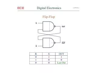
The NOR Gate S-R Latch • The most basic memory element is the S-R LATCH. • The S-R latch has two main inputs: • the Set (S) and the REST (R), and two outputs Q and . ..It has Two-inputs R and S, and two-outputs Q and
From Module 3 • Symbol • circuit diagram • Truth Table • Operation • Exercise Question
Objectives • To know about the operation of Level Triggered Latches. • To understand the function of Clock Signal in SR Latch. • Verify the Truth Table of Level Triggered Latches.
Level Triggered Latches • The Level Triggered latch can be defined as “a logic device that changes its output state in response to a HIGH or LOW level of the clock”; and hence the name Level Triggered latch”.
Clock Signal • A clock signal is applied to decide when a latch is enabled or disabled and when the output changes its state. • The clock signal ensures that the device is triggered into operation at the right time and is denoted with C Clock Signal or EN Enable Signal.
Level Triggered SR latch logic symbol This logic circuit illustrates how S-R latch is modified to add the clock input (CK).
Level Triggered S-R Latch operation • The operation of Level Triggered SR latch is the same as SR Latch except that its output state changes only when the clock level is HIGH.
Operation of Level Triggered S-R Latch • When the level of the clock signal is HIGH (logic-1), the two-AND gates passes the (S and R) inputs through to the latch and the device is enabled. • When the level of the clock signal is LOW (logic-0), the two-AND gates blocks the (S and R) inputs from reaching the latch and the device is disabled. • The when CK is HIGH, the circuit operation is identical to that of the SR latch. The truth table illustrates this operation is shown in Table 7.
Result • inputs to the latch (S and R) are only enabled when the clock signal (CK) is HIGH
Learning Objective • To know about the operation of Level Triggered D-type Latch. • To understand the function of Clock Signal in SR Latch. • Verify the truth Table of Level Triggered D-type Latch. • Difference between the Types of SR Latch.