Download
1 / 46
470 likes | 506 Views
Low-Power Design of Digital VLSI Circuits Power Dissipation of CMOS Circuits. Vishwani D. Agrawal James J. Danaher Professor Dept. of Electrical and Computer Engineering Auburn University, Auburn, AL 36849 vagrawal@eng.auburn.edu http://www.eng.auburn.edu/~vagrawal.

E N D
Low-Power Design of Digital VLSI CircuitsPower Dissipation of CMOS Circuits Vishwani D. Agrawal James J. Danaher Professor Dept. of Electrical and Computer Engineering Auburn University, Auburn, AL 36849 vagrawal@eng.auburn.edu http://www.eng.auburn.edu/~vagrawal Lectures 2, 3, 4: CMOS Circuits
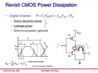
nMOS Logic (Inverters) For logic 1 input, continuous static power is dissipated. Pseudo-nMOS Saturated-load nMOS R. C. Jaeger and T. N. Blalock, Microelctronic Circuit Design, Third Edition, McGraw-Hill, 2006, Chapter 6. Lectures 2, 3, 4: CMOS Circuits
CMOS Logic (Inverter) VDD No current flows from power supply! Where is power consumed? GND F. M. Wanlass and C. T. Sah, “Nanowatt Logic using Field-Effect Metal-Oxide-Semiconductor Triodes,” IEEE International Solid-State Circuits Conference Digest, vol. IV, February 1963, pp. 32-33. Lectures 2, 3, 4: CMOS Circuits
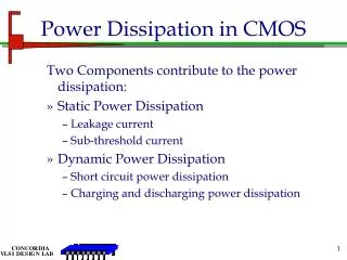
Components of Power • Dynamic • Signal transitions • Logic activity • Glitches • Short-circuit (small) • Static • Leakage Ptotal = Pdyn + Pstat = Ptran +Psc+ Pstat Lectures 2, 3, 4: CMOS Circuits
Power of a Transition: Ptran V = VDD R = Ron i(t) vi (t) v(t) Large resistance C = CL Ground C = Total load capacitance for gate; includes transistor capacitances of driving gate + routing capacitance + transistor capacitances of driven gates; obtained by layout analysis. Lectures 2, 3, 4: CMOS Circuits
Charging of a Capacitor R t = 0 v(t) i(t) C V Charge on capacitor, q(t) = C v(t) Current, i(t) = dq(t)/dt = C dv(t)/dt Lectures 2, 3, 4: CMOS Circuits
i(t) = C dv(t)/dt = [V – v(t)] /R dv(t) V – v(t) ─── = ───── dt RC dv(t) dt ∫───── = ∫ ──── V – v(t) RC – t ln [V – v(t)] = ── + A RC Initial condition, t = 0, v(t) = 0 → A = ln V – t v(t) = V [1 – exp(───)] RC Lectures 2, 3, 4: CMOS Circuits
– t v(t) = V [1 – exp(── )] RC dv(t) V – t i(t) = C ─── = ── exp(── ) dt R RC Lectures 2, 3, 4: CMOS Circuits
Total Energy Per Charging Transition from Power Supply ∞∞ V2 – t Etrans = ∫ V i(t) dt = ∫ ── exp(── ) dt 00 R RC = CV2 Lectures 2, 3, 4: CMOS Circuits
Energy Dissipated per Transition in Resistance ∞ V2∞ – 2t R ∫ i2(t) dt = R ── ∫ exp(── ) dt 0 R20 RC 1 = ─ CV2 2 Lectures 2, 3, 4: CMOS Circuits
Energy Stored in Charged Capacitor ∞ ∞ – t V – t ∫ v(t) i(t) dt = ∫ V [1-exp(── )]─ exp(── ) dt 00 RC R RC 1 = ─ CV2 2 Lectures 2, 3, 4: CMOS Circuits
Transition Power • Gate output rising transition • Energy dissipated in pMOS transistor = CV2/2 • Energy stored in capacitor = CV2/2 • Gate output falling transition • Energy dissipated in nMOS transistor = CV2/2 • Energy dissipated per transition = CV2/2 • Power dissipation: Ptrans = Etransα fck = α fck CV2/2 α = activity factor fck = clock frequency Lectures 2, 3, 4: CMOS Circuits
Components of Power • Dynamic • Signal transitions • Logic activity • Glitches • Short-circuit • Static • Leakage GLITCH Delay=2 2 0 Delay =1 1 3 0 Ptotal = Pdyn+ Pstat = Ptran + Psc+ Pstat Lectures 2, 3, 4: CMOS Circuits
Short Circuit Power of a Transition: Psc VDD isc(t) vi (t) vo(t) CL Ground Lectures 2, 3, 4: CMOS Circuits
Short Circuit Current, isc (t) VDD VDD - VTp n-transistor cuts-off Vi (t) Vo(t) Volt VTn p-transistor starts conducting 0 Iscmaxf isc(t) Isc Time (ns) tB tE 1 0 Lectures 2, 3, 4: CMOS Circuits
Peak Short Circuit Current • Increases with the size (or gain, β) of transistors • Decreases with load capacitance, CL • Largest when CL = 0 • Reference: M. A. Ortega and J. Figueras, “Short Circuit Power Modeling in Submicron CMOS,” PATMOS ’96, Aug. 1996, pp. 147-166. Lectures 2, 3, 4: CMOS Circuits
Short-Circuit Energy per Transition • Escf =∫tBtE VDD isc(t)dt =(tE – tB) Iscmaxf VDD / 2 • Escf= tf(VDD - |VTp|- VTn) Iscmaxf / 2 • Escr= tr(VDD - |VTp| - VTn) Iscmaxr / 2 • Escf= Escr=0, when VDD= |VTp|+ VTn Lectures 2, 3, 4: CMOS Circuits
Short-Circuit Power • Increases with rise and fall times of input. • Decreases for larger output load capacitance; large capacitor takes most of the current. • Small, about 5-10% of dynamic power; momentary shorting of supply and ground during opening and closing of transistor switches. Lectures 2, 3, 4: CMOS Circuits
Short-Circuit Power Calculation • Assume equal rise and fall times • Model input-output capacitive coupling (Miller capacitance) • Use a spice model for transistors • T. Sakurai and A. Newton, “Alpha-power Law MOSFET model and Its Application to a CMOS Inverter,” IEEE J. Solid State Circuits, vol. 25, April 1990, pp. 584-594. Lectures 2, 3, 4: CMOS Circuits
Short Circuit Power Psc = α fck Esc Lectures 2, 3, 4: CMOS Circuits
Psc, Rise Time and Capacitance VDD VDD Ron ic(t)+isc(t) vi (t) vo(t) vo(t) CL tr tf R = large vo(t) ─── R↑ Ground Lectures 2, 3, 4: CMOS Circuits
isc, Rise Time and Capacitance – t VDD[1 – exp (─────)] vo(t) R↓(t) C Isc(t) = ──── = ─────────────── R↑(t) R↑(t) Lectures 2, 3, 4: CMOS Circuits
iscmax, Rise Time and Capacitance i Small C Large C vo(t) vo(t) iscmax 1 ──── R↑(t) t tf Lectures 2, 3, 4: CMOS Circuits
Psc, Rise Times, Capacitance • For given input rise and fall times short circuit power decreases as output capacitance increases. • Short circuit power increases with increase of input rise and fall times. • Short circuit power is reduced if output rise and fall times are longer than the input rise and fall times. Lectures 2, 3, 4: CMOS Circuits
Summary: Short-Circuit Power • Short-circuit power is consumed by each transition (increases with input transition time). • Reduction requires that gate output transition should not be faster than the input transition (faster gates can consume more short-circuit power). • Increasing the output load capacitance reduces short-circuit power. • Scaling down of supply voltage with respect to threshold voltages reduces short-circuit power; completely eliminated when VDD ≤ |Vtp| + Vtn . Lectures 2, 3, 4: CMOS Circuits
Components of Power • Dynamic • Signal transitions • Logic activity • Glitches • Short-circuit • Static • Leakage Lectures 2, 3, 4: CMOS Circuits
Leakage Power VDD IG Ground Gate R Source Drain n+ n+ Isub IPT ID IGIDL Bulk Si (p) nMOS Transistor Lectures 2, 3, 4: CMOS Circuits
Leakage Current Components • Subthreshold conduction, Isub • Reverse bias pn junction conduction, ID • Gate induced drain leakage, IGIDL due to tunneling at the gate-drain overlap • Drain source punchthrough, IPT due to short channel and high drain-source voltage • Gate tunneling, IGthrough thin oxide; may become significant with scaling Lectures 2, 3, 4: CMOS Circuits
Drain to Source Current IDS = μ0 Cox(W/L) Vt2 exp{(VGS –VTH ) / nVt } μ0: carrier surface mobility Cox: gate oxide capacitance per unit area L: channel length W: gate width Vt = kT/q: thermal voltage n: a technology parameter Lectures 2, 3, 4: CMOS Circuits
IDSfor Short Channel Device IDS= μ0 Cox(W/L)Vt2 exp{(VGS –VTH + ηVDS)/nVt} VDS = drain to source voltage η: a proportionality factor W. Nebel and J. Mermet (Editors), Low Power Design in Deep Submicron Electronics, Springer, 1997, Section 4.1 by J. Figueras, pp. 81-104 Lectures 2, 3, 4: CMOS Circuits
Subthreshold Current, Isub • Example: 90nm CMOS inverter • L = 90nm, Wp = 495nm, Wn = 216nm • Temperature 300K (room temperature) • Input set to 0 volt • Vthn = 0.291V, Vthp =0.209V at VDD = 1.2V (nominal) • PTM (predictive technology model) • Spice simulation for leakage current Lectures 2, 3, 4: CMOS Circuits
Subthreshold Current, Isub Lectures 2, 3, 4: CMOS Circuits
Subthreshold Current, Isub Lectures 2, 3, 4: CMOS Circuits
Increased Subthreshold Leakage Scaled device Ic Log (Drain current) Isub 0 VTH’ VTH Gate voltage Lectures 2, 3, 4: CMOS Circuits
Summary: Leakage Power • Leakage power as a fraction of the total power increases as clock frequency drops. Turning supply off in unused parts can save power. • For a gate it is a small fraction of the total power; it can be significant for very large circuits. • Scaling down features requires lowering the threshold voltage, which increases leakage power; roughly doubles with each shrinking. • Multiple-threshold devices are used to reduce leakage power. Lectures 2, 3, 4: CMOS Circuits
CMOS Gate Power v(t) V R = Ron i(t) vi (t) v(t) i(t) Large resistance C isc(t) isc(t) Ground Leakage current time Lectures 2, 3, 4: CMOS Circuits
Technology Scaling • Scaling down 0.7 micron by factors 2 and 4 leads to 0.35 and 0.17 micron technologies • Constant electric field assumed Lectures 2, 3, 4: CMOS Circuits
Constant Electric Field Scaling • B. Davari, R. H. Dennard and G. G. Shahidi, “CMOS Scaling for High Performance and Low Power—The Next Ten Years,” Proc. IEEE, April 1995, pp. 595-606. • Other forms of scaling are referred to as constant-voltage and quasi-constant-voltage. Lectures 2, 3, 4: CMOS Circuits
Bulk nMOSFET Polysilicon Gate Drain W Source n+ n+ L p-type body (bulk) SiO2 Thickness = tox Lectures 2, 3, 4: CMOS Circuits
Technology Scaling • A scaling factor (S ) reduces device dimensions as 1/S. • Successive generations of technology have used a scaling S = √2, doubling the number of transistors per unit area. This produced 0.25μ, 0.18μ, 0.13μ, 90nm and 65nm technologies, continuing on to 45nm, 32nm and 22nm. • A 5% gate shrink (S = 1.05) is commonly applied to boost speed as the process matures. N. H. E. Weste and D. Harris, CMOS VLSI Design, Third Edition, Boston: Pearson Addison-Wesley, 2005, Section 4.9.1. Lectures 2, 3, 4: CMOS Circuits
Constant Electric Field Scaling Lectures 2, 3, 4: CMOS Circuits
Constant Electric Field Scaling(Cont.) Lectures 2, 3, 4: CMOS Circuits
Problem: A Design Example • A battery-operated 65nm digital CMOS device is found to consume equal amounts (P ) of dynamic power and leakage power. The short-circuit power is negligible. The energy consumed by a computing task, that takes T seconds, is 2PT. • Compare two power reduction strategies for extending the battery life: • Clock frequency is reduced to half, keeping all other parameters constant. • Supply voltage is reduced to half. This slows the gates down and forces the clock frequency to be lowered to half of its original (full voltage) value. Assume that leakage current is reduced by a ratio 10/2 = 5 (see slides 32 and 33). Lectures 2, 3, 4: CMOS Circuits
Solution: Strategy A. Clock Frequency Reduction • Reducing the clock frequency will reduce dynamic power to P / 2, keep the static power the same as P, and double the execution time of the task. • Energy consumption for the task will be, Energy = (P / 2 + P ) 2T = 3PT which is greater than the original 2PT. Lectures 2, 3, 4: CMOS Circuits
Solution: Part B. Supply Voltage Reduction • When the supply voltage and clock frequency are reduced to half their values, dynamic power is reduced to P / 8 and static power to P / 10. The time of task is doubled and the total energy consumption is, Energy = (P / 8 + P / 10) 2T = 9PT / 20 =0.45PT • The voltage reduction strategy reduces energy consumption while a simple frequency reduction consumes more energy. Lectures 2, 3, 4: CMOS Circuits
Comparing Strategies A and B Lectures 2, 3, 4: CMOS Circuits