Download
1 / 33
800 likes | 1.75k Views
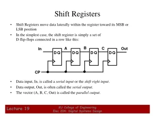
Shift Registers and Shift Register Counters. Week 10 and Week 11 (Lecture 2 of 2). 1 0 0 0. Parallel load a 1000:. Serial receiving device. Q. Q. Q. Q. 0. D. D. D. D. X. X. X. X. 1. 0. 0. 0. 1. C p. C p. C p. C p. CLOCK INPUT. CLOCK. X=Undetermined State.

E N D
Shift Registers and Shift Register Counters Week 10 and Week 11 (Lecture 2 of 2)
1 0 0 0 Parallel load a 1000: Serial receiving device Q Q Q Q 0 D D D D X X X X 1 0 0 0 1 Cp Cp Cp Cp CLOCK INPUT CLOCK X=Undetermined State Shift Register Shift Register is one of the most widely used functional device in Digital Systems. The simple pocket calculator illustrates the shift register’s characteristics. How Shift Register Works ? If a 4-bit shift Register receives 4-bits of parallel data and shift them to the right four positions into some other device STEP-1
1 0 0 0 1 0 0 0 Q Q Q Q Q Q Q Q D D D D D D D D 0 0 0 0 1 0 0 1 0 0 0 0 X X X X X 0 1 1 Apply pulse 1: Apply pulse 2: Cp Cp Cp Cp Cp Cp Cp Cp 2 1 CLOCK CLOCK Shift Register STEP -2 STEP -3
1 0 0 0 1 0 0 0 Q Q Q Q Q Q Q Q D D D D D D D D 1 0 0 0 0 0 0 0 0 0 1 0 0 0 0 0 X 0 1 1 Apply pulse 3: Apply pulse 4: Cp Cp Cp Cp Cp Cp Cp Cp 4 3 CLOCK CLOCK Shift Register STEP - 4 STEP -5
Shift Register One method of identifying Shift Registers is how data is loaded into and read from the storage unit. There are Four Categories of Shift Registers.
Shift Register Serial in/serial out shift register. • Serial entry of data into a shift register. • A 4-bit device implemented with D flip-flop.
1 1 1 1 1 CLK CLK CLK CLK CLK Serial-in/Serial out Shift Register Shift registers are available in IC form or can be constructed from discrete flip-flops as is shown here with a five-bit serial-in serial-out register. Each clock pulse will move an input bit to the next flip-flop. For example, a 1 is shown as it moves across. 1
Input is 01011, lsb in first Shift Register Assumed that the registers is initially cleared. Show the state of the 5-bit register for the specified data input and clock waveforms.
Shift Register Four bits (1010) being entered serially into the register. lsb in first
Serial out –lsb in first Shift Register Four bits (1010) being entered serially into the register. • The register is initially clear. • The 0 is put onto the data input line, when the 1st. Clock pulse, FF0 is reset, thus storing 0. • Next CLK2. Bit 1, is applied to the data input, making D=1 for FF0 and D=0 for FF1, when 2nd. Clock pulse occurs, the 1 on the data input is shifted into FF0, and the 0 was in FF0 is shifted into FF1. • The CLK3. Bit, a 0 is put onto the data input line, and a clock pulse is applied, the 0 is entered into FF0, the 1 stored in FF0 is shifted into FF1, and the 0 stored in FF1 is shifted into FF2. • the CLK4, the last bit, a 1, is now applied to the data input and a clock pulse is applied. This time the 1 is entered into FF0, the 0 stored in FF0 is shifted into FF1, the 1 stored in FF1 is shifted into FF2, and the 0 stored in FF2 is shifted into FF3. • This complete the serial entry of four bits into the shift register.
Four bits (1010) being entered serially into the register. • The bits must be shifted our serially and taken off the q3 output. • After CLK4 in the dta-entry operation, the LSB, 0, appears on the Q3 output. • When clock pulse CLK5, the second bit appears on the Q3 output. • When CLK6, shift the third bits to the output Q3 • When CLK7, shift the fourth bit to the output Q3.
Shift Register A serial in/parallel out shift register. • Figure shows a 4-bit serial in/parallel out shift register and its logic block symbol.
After 4 clock pulses, the data is available at the parallel output. CLK CLK CLK CLK Serial in/parallel out shift register. An application of shift registers is conversion of serial data to parallel form. For example, assume the binary number 1011 is loaded sequentially, one bit at each clock pulse. Parallel out –msb in first
0110, msb in first Shift Register Show the of the 4-bit register for the data input and clock waveforms. The register initially contains all 1’s. The register contains 0110 after 4 clock pulses.
Shift Register A 4-bit parallel in/serial out shift register.
Shift Register A 4-bit parallel in/serial out shift register. • There are four data-input lines, D0, D1, D2, D3 and a SHIFT/LOAD input, which allows four bits of data to load in parallel into the register. • When SHIFT/LOAD is LOW, gates G1 through G3 are enabled, allowing each data bit to be applied to the D input of its respective flip-flop. • When a clock is applied, the flip-flops with D=1 will set and those with D=0 will reset, thereby storing all four bits simultaneously. • When SHIFT/LOAD is HIGH, gates G1 through G3 are disabled and G4 through G6 are enabled, allowing the data bits to shift right from one stage to the next. • The OR gates allow either the normal shifting operation or parallel data-entry operation, depending on which AND gates are enabled by the level on the SHIFT/LOAD input.
Shift Register Show the data-output waveform for a 4-bit register with the parallel input data and the clock and SHIFT/LOAD waveforms given. Parallel out – msb first out
Shift Register A parallel in/parallel out register.
Shift Register • The 74HC195 can be used for parallel in/parallel out operation. It also can be used for serial in/serial out and serial in/parallel out operation.
Shift Register • It can be used for parallel in/parallel out by using Q3 as the output. • When the SHIFT/LOAD input is LOW, the data on the parallel inputs are entered synchronously on the positive transition of the clock. • When SHIFT/LOAD is HIGH, stored data will shift right (Q0 to Q3) synchronously with the clock. • Inputs J and K are the serial data inputs to the first stage of the register (Q0); Q3 can be used for serial output data. • The active-LOW clear input is asynchronous.
Shift Register Sample timing diagram for a 74HC195 shift register.
Shift Register 4-Bit Bidirectional Shift Register-Logic Diagram
Shift Register 4-Bit Bidirectional Shift Register-Operation • A HIGH on the control input allows data bits inside the register to be shifted to the right and a LOW enables data bits inside the register to be shifted to the left. • When the control input is HIGH, gates G1 through G4 are enabled, and the state of the Q output of each flip-flop is passed through to the D input of the following flip-flop. When a clock pulse occurs, the data bits are shifted one place to the right. • When the control input is LOW, gates G5 through G8 are enabled, and the Q output of each flip-flop is passed through to the D input of the preceding flip-flop. When a clock pulse occurs, the data bits are then shifted one place to the left.
Shift Register 4-Bit Bidirectional Shift Register-Timing Diagram Assume that initially Q0=1, Q1=1, Q2=0, and Q3=1 and the serial data-input is LOW. Timing diagram for the given control input waveform is given below:
The Johnson Counter • A Johnson counter will produce a modulus of 2n. • A 4-bit device has a total of 8 states and the 5-bit device has a total of 10 states. • The implementation of a Johnson counter is the same regardless of the number of stages. • The Q output of each stage is connected to the D input of the next stage, except the Q output of the last stage is connected back to the D input of the first stage.
The Johnson Counter Four-bit Johnson sequence:
The Johnson Counter Five-bit Johnson sequence:
The Johnson Counter Timing sequence for a 4-bit Johnson counter
The Johnson Counter • Timing sequence for a 5-bit Johnson counter
The Ring Counter • Logic diagram for a 10-bit ring counter. • The inter-stage connections are the same as those for a Johnson counter, except that Q rather than Q is fed back from the last stage.
The Ring Counter 10-bit ring counter sequence
The Ring Counter If a 10-bit ring counter has the initial state 1010000000, determine the waveform for each of the Q outputs.