Download
1 / 46
510 likes | 809 Views
4-4-3 Shift registers. Learning Objectives: At the end of this topic you will be able to; i) recognise, analyse and design circuits containing D-type flip-flops to form parallel-in-serial-out (PISO) registers, and serial-in-parallel-out (SIPO) registers; ii)draw timing diagrams.

E N D
Learning Objectives: At the end of this topic you will be able to; i) recognise, analyse and design circuits containing D-type flip-flops to form parallel-in-serial-out (PISO) registers, and serial-in-parallel-out (SIPO) registers; ii)draw timing diagrams.
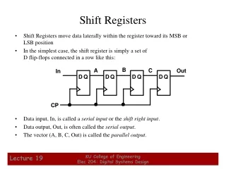
Shift Registers In Module ET1 we introduced the D-Type Flip Flop and demonstrated how it could be used as a counter. In this topic we will develop another application of the D-Type Flip-Flop, that is the shift register. A shift register is a very important functional unit in modern digital systems, as it is used for helping to move data from one system to another. More importantly it is able to swap data transfer from serial to parallel, or parallel to serial. This will be extremely important when we meet our next topic 4.5.4 – Pulse Code Modulation, however for now we will focus just on the operation of the shift register. First we will look at the two types of communication.
Serial Transfer: In serial transfer, data is moved along a single data line from one location to another, one bit at a time, the process can be slow, but only has to carry one signal along one pair of wires in the connecting cable, and therefore is very economical to make. Parallel Transfer: In parallel data transfer, the data is moved along multiple data paths at the same time, in the case shown above, 8 bits are moved at the same time. Data transfer is quick, but the cable has to be able to carry 8 signals along 8 pairs of wires in the cable at the same time and is therefore much more expensive than serial transfer.
Note: Advances in modern techniques now enable serial communication links to operate at near the same rate as parallel links. e.g. modern USB2 Serial links operate at very high speeds, giving the data transfer rate of a parallel link in serial form. The shift register is a functional unit which acts as an interface to allow data to be transferred from a serial to parallel or from parallel to serial systems. We will now look at how these interfaces can be constructed from D-Type Flip Flops. The first type we will look at is the Serial-In-Parallel-Out (SIPO). The circuit required is as follows: Output A Output B Output C Output D SA DA QA Data In SB SC SD QB DC DD DB QD QC RA Clock RB RC RD Reset QA QC QD QB
At first glance you might think that this is the circuit for a counter, and indeed in examinations a significant number of candidates think it is and draw timing diagrams suitable for a counter, quite incorrectly of course! There are a couple of observations to be made about this circuit which clearly separate it from the counter circuits encountered in ET1 i.The clock signal is common to each D-Type, so they are all clocked at the same time. ii.The Q-output of each D-Type is connected to the D-input of the next flip-flop in the chain. iii.The output of each D-Type is not connected. Q Looking out for these three characteristics should help you to distinguish the shift register from the counter.
This type of shift register takes in serial data through the DIN terminal, and parallel data is available at Output A, B, C and D. Other control circuitry which is not shown ensure that the correct number of clock pulses are received to transfer the data in and out of the shift register. In this particular case there are 4 clock pulses required to transfer four bits of data from the serial input to the parallel outputs. Larger shift registers are available and can be made quite easily just by linking more D-Type flip-flops into the chain. We usually encounter four types of question related to Shift registers. 1.Registers connected via logic gates to other registers. 2.Drawing timing diagrams for shift registers. 3.Completing tables to show the status of self filling shift registers. 4.Complete a diagram to show how a SIPO shift register is connected, from a block diagram of un-connected D-Type flip-flops.
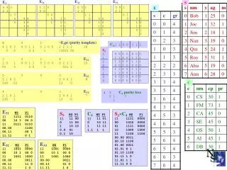
Register A Register A 1 1 1 1 0 0 0 0 1 0 0 1 0 0 Output Register Output Register 0 0 Register B Register B 1.If we consider the first case, this is probably the most straightforward. You will be presented with a diagram similar to the one shown below. Complete the diagram below to show the content of the registers after 4 clock pulses.
Register A 1 1 0 0 1 0 1 0 1 0 0 1 0 Output Register 0 Register B Registers A and B are straightforward, as these will fill with Logic 1 and Logic 0, respectively. You will need to remember your logic gates from ET1 to complete the output register. You should remember that the NOR gate gives an output of logic 1 when both inputs are at logic 0. The final diagram therefore becomes:
2.Now we will look at how to construct a timing diagram for the shift register. We are usually presented with a diagram similar to the one below to start. Clock DIN QA QB QC QD
At first it might appear a little daunting as how to proceed with the completion of such a large number of diagrams. The trick is to focus initially on the output for QA. You should remember from ET1 that the logic level of DIN is transferred to the Q output on the rising edge of the clock pulse. Note that all of the outputs have been reset to Logic 0. If we only consider the output QA, to start with, the output for the given DIN signal will be as shown below.
Clock DIN QA QB QC QD
Clock DIN QA QB QC QD Now that the first output has been completed, the remaining outputs will be quite easy to complete, since QA becomes the input for DB, and will be transferred to QB at the next clock pulse.
Clock DIN QA QB QC QD The remaining outputs are completed in the same way, since QB becomes the input for DC, and will be transferred to QC at the next clock pulse etc.
This completes the diagram, the outputs for QB, QC and QD follow on from each other, the most important output to obtain is QA, so great care should be taken completing this particular output.
S S S S A B D C Q Q Q DIN DIN DIN DIN Q R R R R Reset Clock 3. The third way in which shift registers appear in questions is the self-filling register which uses a logic gate to use some of the register bits to generate the next input bit. This is illustrated below. Q Q Q Q
The counter is initially reset, so that outputs A, B, C and D are all at logic 0. Complete the following table to show the output for successive clock pulses. In this case the clock sequence was consecutive, however in an exam some steps may be left out. You will see an example of this in the student exercise.
Output C Output B Output D Output A S S S S Q DIN DIN DIN DIN Q Q Q Input Reset R R R R Clock 4.The final type of question would be to complete a circuit diagram for a SIPO shift register from a basic block diagram as shown below. You will be given a circuit like this: Q Q Q Q
The diagram needs to be completed by adding the connections shown by the red lines below:
Parallel-In-Serial-Out Shift Register The basic layout of the PISO shift register is very similar to that of the SIPO, and care must be taken to ensure that you do not get the two mixed up. There are a number of different versions of the PISO circuit but for the purposes of this course the only one that will be used is as shown below.
The process of loading the register with data is as follows. When first switched on the D-types are reset by pulsing the reset line to reset the output of all the D-types to logic 0. i) The data is then put on the data lines D3, D2, D1, and Do. ii) The ‘load’ line is then taken to logic 1, which allows any logic 1, present on the D3, D2, D1, and Do lines to SET the output of the corresponding D-Type to a logic 1. The load line is then taken back to Logic 0. iii) The clock line then pulses four times to move the data out of the shift register. iv) As DIN of the first D-Type is connected to logic 0, there will be no need to reset the D-Types at the end of the 4 clock pulses as all D-Types will contain logic 0, ready for the next time data is loaded into the register.
Questions about the PISO shift register will be related to the following: 1. Complete a timing diagram for the shift register. 2. Complete an un-connected diagram of D-type flip-flops to make a PISO. We fill first consider the possibility of completing a timing diagram for the PISO. We start with a circuit diagram giving the logic levels of the parallel input data.
The timing diagrams applied to the Reset, Load, and Clock are shown on the following page. Complete the timing diagrams for QA,QB, QC, and QD.
Reset Load Clock QB QC This is the way in which the timing diagram would be presented in the examination. We will now consider stage by stage what happens as the signals are applied. Note that QA,QB, QC, and QD, have been given some initial value.
Reset Load Clock QB QC The first signal to have any effect on the outputs of QA, QB, QC and Qwill be the reset pulse which will reset all outputs to logic 0 as shown.
Reset Load Clock QB QC Next will be the effect of the ‘Load’ signal, which will set the outputs to the state of the parallel inputs, as shown in the original circuit diagram, as shown below.
Reset Load Clock QB QC The data has now been loaded into the Shift register, so now the clock pulses take over to move the data through, the register. The input to the register is set to logic 0 so this keeps moving in logic 0 at the input with every clock pulse. After one clock pulse we have.
Reset Load Clock QB QC At the next clock pulse these diagrams will look like the following:
Reset Load Clock QB QC And then after clock pulse 3, the graph would look like this.
Reset Load Clock QB QC 0 1 1 0Data Out If the inputs have been left unchanged from the circuit diagram, then the timing diagram would be completed as follows:
The data has now been shifted out of the register and all outputs have been set to logic 0, ready for the next parallel load pulse. Notice that four clock pulses are required to empty the register and ensure that all bits are set to logic 0 prior to the ‘load’ line going high to enter the next four bits of data into the register. The completion of the timing diagram is a little more involved than a SIPO and care should be taken when drawing this type of diagram. The control circuitry used to synchronise the reset, load and clock signals is complex and is not covered in this syllabus.
The second type of question for the PISO is to complete the drawing of the circuit as shown on page 13. You will find an example of this in the following student exercise which will include questions on both SIPO and PISO shift registers.
Clock DIN QA QB QC QD
Complete the timing diagrams opposite to show how the outputs change in relation to the applied signals.
Reset Load Clock QB QC
Solutions to Student Exercise. Student Exercise 1.