Download
1 / 47
530 likes | 666 Views
EMT 272 Semiconductor Fundamentals SEMICONDUCTOR PHYSICS Carrier Transport Phenomena. Outlines:. Carrier Drift Carrier Diffusion Generation & Recombination Process Continuity Equation Thermionic Emission Process Tunneling Process High-Field Effect. Part 2:. Continuity Equation

E N D
EMT 272 Semiconductor FundamentalsSEMICONDUCTOR PHYSICSCarrier Transport Phenomena
Outlines: • Carrier Drift • Carrier Diffusion • Generation & Recombination Process • Continuity Equation • Thermionic Emission Process • Tunneling Process • High-Field Effect
Part 2: • Continuity Equation • Thermionic Emission Process • Tunneling Process • High-Field Effect
Continuity Equation • The continuity equation satisfies the condition that particles should be conserved! Electrons and holes cannot mysteriously appear or disappear at a given point, but must be transported to or created at the given point via some type of carrier action. • Inside a given volume of a semiconductor, • There is a corresponding equation for electrons.
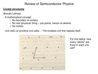
Continuity Equation • Consider overall effect when drift, diffusion and recombination occur simultaneously in a semiconductor material. To derive 1D continuity equations for electrons, consider an infinities-imal slice with a thickness dx located at x shown in figure.
The number of electron in the slice – increase due to net current flow into the slice & the net carrier generation in the slice. • The OVERALL RATE OF ELECTRON increase is algebraic sum of 4 components: A – B + C – D where; A = number of electrons flowing into the slice at x B = number of electrons flowing out at x + dx C = rate which electrons are generated D = rate at which they are recombined with holes in the slice
The overall rate of change in the number of electrons in the slice: (1) where, A : cross section area, Adx: volume of the slice • For 1-D, under low injection condition, the BASIC CONTINUITY EQUATION FOR MINORITY CARRIERS: (2) ELECTRONS HOLES
In addition to continuity equations, Poisson’s equation: (3) must be satisfied, and s – s/cond dielectric permittivity, s – space charge density, where s = q(p – n + ND+ - NA-)
Carrier Concentration Notation • The subscript “n” or “p” is used to explicitly denote n-type or p-type material, e.g. • pn is the hole (minority-carrier) concentration in n-type material • np is the electron (minority-carrier) concentration in n-type material • Thus the minority carrier diffusion equations are
CONTINUITY EQUATION GENERATION-RECOMBINATION DIFFUSION DRIFT LIGHT
Simplifications (Special Cases) • Steady state: • No diffusion current: • No R-G: • No light:
Solve Continuity Equations • Steady State Injection From One Side • Minority Carriers at the Surface • Haynes Shockley Experiment
STEADY STATE INJECTION FROM ONE SIDE Consider excess carriers are injected from one side to n type s/cond as result of illumination. Assume steady state and no light adsorption at x>0. Thus, light 0 x is diffusion length
The general solution to the equation Therefore, the solution is (5)
light 0 W • With thickness x = W, thus (6) Where, CURRENT DENSITY at x = W is given by (7)
MINORITY CARRIERS AT THE SURFACE • When surface recombination is introduced, the hole current density flowing into the surface from the bulk of the s/cond. It’s given by qUs. • Assume that the sample is uniformly illuminated with uniform generation of carriers and at steady state. • Surface recombination leads to a lower carrier concentration at the surface. The gradient of hole concentration yield a diffusion current density that is equal to the surface recombination current. • The solution of the continuity equation based on boundary condition (x = 0, and x = ), is (8) When Slr 0, thus, When Slr , thus, (9) Slr: low injection surface recombination velocity
Surface recombination at x = 0. The minority carrier distribution near the surface is affected by the surface recombination velocity.
HAYNES SHOCKLEY EXPERIMENT • One of the classic experiments in semiconductor physics to demonstrate drift • and diffusion of minority carriers (mobility and diffusion coefficient). Phys. Rev. Vol 81 pg. 835 (1951)
The voltage source V1 establishes • an electric field in the +x direction in • the n-type semiconductor bar. • Excess carriers are produced and • effectively injected into the • semiconductor bar at Contact (1) • by a pulse. • Contact (2) may collect a fraction • of the excess carriers as they drift • through the s/cond. The Hayes-Shockley experiment. (a) Experimental setup. (b) Carrier distributions without an applied field. (c) Carrier distributions with an applied field. Without applied field Carrier distributions With applied field
After a pulse, by setting Gp = 0, and E/x = 0 (applied electric is constant across the conduction bar), thus transport equation is given by: (10) And the solution may be written as (11) For no electric field applied along the sample, = x (refer figure b), and with electric field, = x - pEt (refer figure c). N = number of electrons or holes generated per unit area. For E = 0, carriers diffuse away from the point of injection and recombine. For E 0, all excess carriers move with drift velocity pE, and diffuse outward and recombine as in the field-free case.
Thermionic Emission Process • Previously, we consider carrier transport inside bulk s/cond and at the s/cond surface, carriers may recombine with recombination centers due to the dangling bonds of the surface region. • BUT WHEN • THERMIONIC EMISSION PROCESS– condition where the carriers have sufficient energy to ‘thermionically’ emitted into the vacuum. Thus, the electrons are emitted across a barrier. • This occurs because the thermal energy given to the carrier overcomes the binding potential, also known as work function.
q- electron affinity is the energy difference between the conduction band edge & the vacuum level in the s/cond. • qs – work function (energy between Fermi level & vacuum level in the s/cond). • If energy > q - electron can be thermionically emitted into the vacuum. (a) The band diagram of an isolated n-type semi-conductor. (b) The thermionic emission process. (a) (12) • ELECTRON DENSITY WITH ENERGY> q • may be written as : (b) NC – effective density of states in cond. band. Vn – is the difference between bottom of cond. band & Fermi level.
EXAMPLE • Calculate the thermionically emitted electron density, nth at room temperature (300K) for n type silicon sample with electron affinity, q = 4.05 eV and qVn = 0.2 eV. If we reduce the effective q to 0.6 eV, what is the nth? Critic the answer. • SOLUTION Nth (4.05 eV) = 2.86 x 10¹⁹ exp(-[4.05 + 0.2/0.0259]) = 2.86 x 10¹⁹ exp (-164) = 10-52 = 0 Nth (0.6 eV) = 2.86 x 10¹⁹ exp(-[0.6 + 0.2/0.0259]) = 2.86 x 10¹⁹ exp (-30.9) = 1 x106 cm-3 From the answer, at room temperature no emission of electrons into vacuum for q = 4.05 eV. But when we lower the q to 0.6 eV, number of electrons can be thermionically emitted.
Tunneling Process • QUANTUM TUNNELING PHENOMENA: • The energy diagram when two • isolated s/cond samples are brought close together. The distance between them is d, the potential barrier height qVo is equal to electron affinity q. • If d<<<, electron at left-side s/cond may transport across the barrier & and move to the other side (even if electron energy is less than barrier height.) (a) The band diagram of two isolated semiconductors with a distance d. (b) One-dimensional potential barrier. (c) Schematic representation of the wave function across the potential barrier.
Classic case: particle is always reflected (if E < qVo). • Quantum case: particle has finite probability to transmit or ‘tunnel’ through the potential barrier. • The behavior of particle (conduction electron) in the region with qV(x) = 0 can be described by Schrödinger equation: (13) • Where mn – effective mass, ħ - reduced Planck constant, E – kinetic energy, and - wave function of the particle. • The solution of (13) are (14) Where k = (2mnE/ħ2)1/2.
For x 0 : incident-particle wave function with amplitude A and reflected wave function with amplitude B. For x d : transmitted wave function with amplitude C. • Inside the potential barrier, wave function may be written as (15) The solution of E < qVo: (16) Where = {2mn(qVo – E)/ħ2}1/2. (x) illustrated at Figure (c).
Transmission coefficient may be written as (17) Transmission coefficient decreases as E decreases. When d >> 1, (C/A) <<< and varies as (18) For finite transmission coefficient, we need small d, low potential barrier qV and small effective mass, m * Used for tunneling diodes in the next chapter
High Field Effects • At low electric field, drift velocity is proportional to the applied field, and assume that time interval between collision c is independent of the applied field. (Assumption for drift velocity < thermal velocity of carrier, 107 cm/s for Si at room temperature). • As the drift velocity reach thermal velocity, its field dependence on the electric field will depart from linear relationship. • Drift velocity increases less rapidly when electric field increased. At large field, the drift velocity approaches a saturation velocity. Drift velocity: (19) Where vs – saturation velocity (107cm/s for Si at 300K). E0 – constant field which is 7 x 10³ V/cm for electrons and E0 = 2 x 10⁴V/cm for holes in high-purity Si materials. - 2 for electrons and 1 for holes.
shows the measured drift velocity of electrons and holes in Si as a function of the electric field. • Drift velocity increases less rapidly when electric field increased. • At large field, the drift velocity approaches a saturation velocity. Drift velocity versus electric field in Si.
shows the differentiation between high-field transport in n-type GaAs and Si. • For n-type GaAs – vs reached maximum level, then decreases when the field increases. This phenomenon is due to energy bands structure of GaAs that allows the transfer of conduction electrons from high mobility energy minimum (called valley) to low mobility. • Means that, electron transfer from the central valley to the satellite valleys along [111] direction. Drift velocity versus electric field in Si and GaAs. Note that for n-type GaAs, there is a region of negative differential mobility.
Next figure gives a clear view of the phenomena, where it considers the simple two-valley model of n-type GaAs at various conditions of electric fields. • Energy separated between two-valleys is E = 0.31eV. The lower valley’s electron effective mass, electron mobility, and electron density are represented by m1, 1, and n1 respectively. The upper level represents by the same expression with subscript 2. • At Figure (a), E << and all electrons remain in the lower valley. • Figure(b), E is higher and some electrons gain sufficient energies from the field to move to the higher valley. • Figure c), E >>, it may transfer all electrons to the higher valley.
Total electron concentration is given by n = n1 + n2. The steady-state conductivity of n-type GaAs may be written as • The average mobility is • Drift velocity may be written as (20) (21) (22)
Electron distributions under various conditions of electric fields for a two-valley semiconductor.
At Figure (a), E << and all electrons remain in the lower valley. • Figure(b), E is higher and some electrons gain sufficient energies from the field to move to the higher valley. • Figure c), E >>, it may transfer all electrons to the higher valley. • In mathematical view; • For 0 < E < Ea • Ea < E < Eb • E > Eb • The drift velocity: • For 0 < E < Ea • For E > Eb and (23) and and (24)
One possible velocity-field characteristic of a two-valley semiconductor. • If 1E > 2E – there is a region which the vs decreases with an increasing field at • Ea < E < Eb • With this characteristic of n-type GaAs drift velocity – this materials is used in microwave transferred-electron devices
When E in s/cond is increased above a certain value – the carriers gain enough kinetic energy to generate electron-hole pairs by an avalanche process shown in (electron in cond. band represented by 1). • If E >>> - electron can gain kinetic energy before it collides with the lattice. • On impact with the lattice – electrons imparts most of its kinetic energy to break a bond – to ionize a valence electron from the valence band to the cond. band & generate an electron-hole pair (represented by 2 and 2’). • This process continued to generate another electron-hole pairs (represented by 3 and 3’, 4 and 4’) and so on. This process called AVALANCHE PROCESS (impact ionization process). Energy band diagram for the avalanche process.
Consider the process of 2 – 2’: • Just prior to the collision, fast moving electron (no. 1) has a kinetic energy = ½ m1vs2, and momentum, p = m1vs, (m1 – effective mass). • After collision, there are 3 carriers: the original electron + electron hole pair (no.2 and 2’). If we assume the 3 carriers have same effective mass, same kinetic energy, and same p, thus: TOTAL KINETIC ENERGY = 3/2 (m1vf2), and TOTAL p = 3m1vf. vf - velocity after collision. • To conserve both energy and momentum before and after the collision, thus and (25) respectively (26)
Eg – band gap corresponding to the minimum energy required to generate an electron-hole pair. By substitute (26) into (25), thus the REQUIRED KINETIC ENERGY FOR IONIZATION PROCESS may be written as • E0 > Eg for the ionization process to occur. It depend on the band structure, where for Si, electron and hole are E0 = 3.6eV (3.2Eg) and E0 = 5.0eV(4.4Eg) respectively. • The number of electron-hole pairs generated by an electron per unit distance traveled – ionization rate, where for the electron and hole is represented by n and p respectively. (27)
Measurement of ionization rates for Si and GaAs are shown in figure. (n and p are strongly dependent on the electric field.) • For large ionization rate (e.g. 104cm-1), the corresponding electric field is 3 x 10⁵ V/cm for Si and 4 x 10⁵ V/cm for GaAs. • ELECTRON HOLE PAIR GENERATION RATE, GAfrom the avalanche process is given by (28) Measured ionization rates versus reciprocal field for Si and GaAs. Where Jn and Jp are the electron and hole current densities, respectively. This expression may be used in the continuity equation for devices operated under the avalanche condition.
EXAMPLE Consider the process of 2’ to 2 during avalanche process, proof that the kinetic energy required for ionization is: SOLUTION The fast moving electron (no. 1) has a kinetic energy = ½ m1vs2, and momentum, p = m1vs. After collision, there are 3 carriers: the original electron + electron hole pair (no.2 and 2’). If we assume the 3 carriers have same effective mass, same kinetic energy, and same p, thus: TOTAL KINETIC ENERGY = 3/2 (m1vf2), and TOTAL p = 3m1vf. vf - velocity after collision. To conserve both energy and momentum before and after the collision,
And Thus,
SUMMARY • Continuity equation – the governing equation for the rate of charge carriers. • Thermionic emission occurs when carriers in the surface region gains enough energy to be emitted into vacuum level. • Tunneling process – based on the quantum tunneling phenomena that results in the transport of electrons across a potential barrier even if the electron energy is less than the barrier height. When the electric field become higher, drift velocity departs from its linear relationship with the applied field & approaches a saturation velocity. • Impact ionization or avalanche process – high field accelerates a new electron-hole pairs, which collide with the lattice to create more electron-hole pairs. From avalanche process, the p-n junction breaks down and conducts a large current
NEXT TOPIC: p-n junction