Download
1 / 35
350 likes | 357 Views
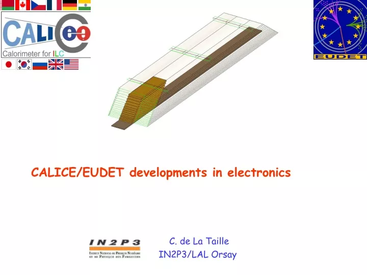
CALICE/EUDET developments in electronics. C. de La Taille IN2P3/LAL Orsay. 3 ×15 cells. Short detector slabs (14). Long detector slab (1). Complete Tower of 4 wafers = 18 ×18 cm 2. Overview. 1st generation front-end electronics in beam : physics prototypes Validate Imaging calorimetry

E N D
CALICE/EUDET developments in electronics C. de La Taille IN2P3/LAL Orsay
3×15 cells Short detector slabs (14) Long detector slab (1) Complete Towerof 4 wafers = 18×18 cm2 Overview • 1st generation front-end electronics in beam : physics prototypes • Validate Imaging calorimetry • ECAL, AHCAL, coming up (US) DHCAL • Running since 2004 • 2nd generation VFE : EUDET R&D : technological modules • Show feasibility for large dimensions • Embedded electronics • Ultra low power in pulsed mode • On chip zero-suppress • Industrializable • EUDET : ECAL, AHCAL for 2009 • ANR : DHCAL • 3rd generation VFE • All features validated • Critical issues : ADC, power pulsing TCMT 120 cm 90 cm ECAL beam C. de La Taille CALICE VFE Developments SOCLE Clermont
Common DAQ Slice FE FPGA Conf/ Clock Clock+Config+Control • Very high integration • No external components system on chip • No active cooling power pulsing for ultra low consumption VFE ASIC VFE ASIC VFE ASIC VFE ASIC PHY Data DIF • Timing is the same for all detectors • Number of channels involves embedded electronic for all detectors • Outputting of data is done the same way for all detectors • Back-end of very-front-end shall be common for all detectors Concentrator (LDA) Detector Interface (DIF) Detector VFE Asic BE of VFE FE of VFE C. de La Taille CALICE VFE Developments SOCLE Clermont
Read out : token ring 1 event 5 events 3 events 0 event 0 event Chip 0 Chip 1 Chip 2 Chip 3 Chip 4 Data bus Chip 0 A/D conv. DAQ IDLE MODE Acquisition Chip 1 A/D conv. IDLE DAQ IDLE MODE Acquisition Chip 2 A/D conv. IDLE IDLE MODE Acquisition Chip 3 A/D conv. IDLE IDLE MODE Acquisition Chip 4 A/D conv. IDLE DAQ IDLE MODE Acquisition C. de La Taille CALICE VFE Developments SOCLE Clermont
EUDET ROC ASICs[J. Fleury et al.] HaRDROC SKIROC SPIROC
The front-end ASICs : the ROC chips SPIROC Analog HCAL (SiPM) 36 ch. 32mm² June 07 HARDROC Digital HCAL (RPC, µmegas or GEMs) 64 ch. 16mm² Sept 06 SKIROC ECAL (Si PIN diode) 36 ch. 20mm² Nov 06 C. de La Taille CALICE VFE Developments SOCLE Clermont
Block scheme of a ROC chip Only in analog read-out chip (SKIROC, SPIROC) 36-channel Wilkinson ADC Event builder Main Memory SRAM Analog channel Analog mem. Ch. 0 Analog channel Analog mem. Ch. 1 xCAL SLAB Analog channel Analog mem. Ch. 35 24 bit counter Time digital mem. Bunch crossing Com module Trigger control Memory pointer C. de La Taille CALICE VFE Developments SOCLE Clermont
HaRDROC chip for DHCAL [LAL,IPNL] JRA3 Milestone • Hadronic Rpc Detector Read Out Chip (Sept 06) • 64 inputs, preamp + shaper+ 2 discris + memory + Full power pulsing • Compatible with 1st and 2nd generation DAQ : only 1 digital data output Discris Digital memory 64 Analog Channels Dual DAC Bandgap Control signals and power supplies C. de La Taille CALICE VFE Developments SOCLE Clermont
Scurves of the 64 channels 30 fC 10 fC Piedestal After Gain correction Dac unit Dac unit C. de La Taille CALICE VFE Developments SOCLE Clermont
HARDROC : first results on Power pulsing PWR ON DAC output (Vth) Trigger Trigger 2 µs 25 µs ZOOM • PWR ON: ILC like (1ms,199ms) • All decoupling capacitors removed • PP of the analog part: • Input signal synchronised on PWR ON • Injection of 100fC, Threshold= 30fC • => Awake time= 2 µs • Power pulsing of the DAC: • 25 µs (slew rate limited) C. de La Taille CALICE VFE Developments SOCLE Clermont
First Daisy chain measurement • First measurement of four chips on the DHCAL prototype PCB (IPNL, LLR, LAL) C. de La Taille CALICE VFE Developments SOCLE Clermont
SKIROC for W-Si ECAL • Silicon Kalorimeter Integrated Read Out Chip (Nov 06) • 36 channels with 16 bits Preamp + bi-gain shaper + autotrigger + analog memory + Wilkinson ADC • Digital part outside in a FPGA for lack of time and increased flexibility • Technology SiGe 0.35µm AMS. Chip received may 07, tests starting 1 MIP in SKIROC C. de La Taille CALICE VFE Developments SOCLE Clermont
SPIROC overview JRA3 Milestone • Silicon Photomultiplier Integrated Read Out Chip • A-HCAL read out • Silicon PM detector • G = 3 E5 to 1 E6 • Same biasing scheme as TB • 36 channels • Charge measurement (15bits) • Time measurement (< 1ns) • Compatible with old & new DAQ • Complex chip,, but many SKIROC, HARDROC, and MAROC features re-used • Submitted june 11th • Expected september C. de La Taille CALICE VFE Developments SOCLE Clermont
ValidHoldAnalogb gain gain Wilkinson ADC Discri output Wilkinson ADC Discri output Trigger discri Output Trigger discri Output Conversion ADC + Ecriture RAM RAM 16 RazRangN Chipsat 16 ReadMesureb 16 Acquisition NoTrig ExtSigmaTM (OR36) StartAcqt SlowClock Hit channel register 16 x 36 x 1 bits TM (Discri trigger) BCID 16 x 8 bits 36 Channel 0 StartConvDAQb 36 ValGain (low gain or high Gain) TransmitOn readout RamFull OutSerie 36 EndReadOut EndRamp (Discri ADC Wilkinson) StartReadOut Rstb FlagTDC Channel 1 Clk40MHz ..… ADC ramp Startrampb (wilkinson ramp) OR36 … StartRampTDC TDC ramp ChipID Chip ID register 8 bits 8 ValDimGray DAQ ASIC ValDimGray 12 bits 12 C. de La Taille CALICE VFE Developments SOCLE Clermont
Conclusion • The three calorimeters have a FE ASIC • HARDROC for the DHCAL • SPIROC for the AHCAL • SKIROC for the ECAL • Some crucial points have been validated • Digital daisy-chain • Power Pulsing • Stand-alone capability (ne external component) • The production is foreseen mid’08 • Very agressive schedule • Still in the EUDET milestones C. de La Taille CALICE VFE Developments SOCLE Clermont
A 35mW 12 bits 25 MS/s pipelined analog to digital converter IN2P3 / LPSC Grenoble -FRANCE • High speed => more than 25Mhz • High dynamique: 2V over a 3.3V power supply • Full differential CMOS design • Low power consumption:1.4mW/MSPs • Fast power pulsing C. de La Taille CALICE VFE Developments SOCLE Clermont
12 bits Slow ADC 12 bits Slow ADC 12 bits Slow ADC 12 bits Slow ADC 12 bits Slow ADC Shaper_1 Shaper_1 Shaper_1 Shaper_1 Shaper_1 Memory Memory Memory Memory Memory preamp preamp preamp preamp preamp Memory Memory Memory Memory Memory Shaper_10 Shaper_10 Shaper_10 Shaper_10 Shaper_10 Shaper_1 Shaper_1 Shaper_1 Shaper_1 Shaper_1 Memory Memory Memory Memory Memory preamp preamp preamp preamp preamp Memory Memory Memory Memory Memory Shaper_10 Shaper_10 Shaper_10 Shaper_10 Shaper_10 Slow versus fast digitizer for CALICE Which one will optimize better: Power / Clock noise / cross talk 12 bits Fast ADC 12 bits Fast ADC C. de La Taille CALICE VFE Developments SOCLE Clermont
Die photographe of the prototype Oct.07 A 1.5 bits stage Error Correction S&H stage Power pulsing C. de La Taille CALICE VFE Developments SOCLE Clermont
Linearity results The Clock noise in S&H (layout problem) leads to this high INL; it is fixed and better results expected for December DNL good but=> will be improved by capacitors DEM C. de La Taille CALICE VFE Developments SOCLE Clermont
Noise-Free Transfer Curve Average output code Probable Output Transfer Curve Code Edge Locations Input Noise Probability Density DC input Code-Edge Noise results @25Mhz .8 LSB for SH+ADC Means .8/√2 for ADC alone Let’s say : .8 LSB C. de La Taille CALICE VFE Developments SOCLE Clermont
Bias pulsing: Data output point of view =>16 to 20µs C. de La Taille CALICE VFE Developments SOCLE Clermont
Spectral response to an input sinus:1Mhz, 2V pp Many harmonics=> layout problem from the switch's Vdd in the S&H Dynamic range >80db 2V Output reconstructed signal Output codes histogram; no missing code C. de La Taille CALICE VFE Developments SOCLE Clermont
Comments on results from this12 bits ADC • The DC power consumption is exactly fitting with our simulations: 35mW for S&H (simplified memory) + ADC • No Obviousmissing codes;σ=0.8LSB for SH+ADC • We cover a good dynamic range: 2V PP @3.3V supply • The sampling speed more than25MS/s. • Tested @35MHzbut then missing codes found due to dutycycle problem in theLVS clock translator=> we fixed it. • The very fast power pulsing, actual delay=>16µs, with a standby efficiency better than 1/1000. • Harmonics & INL=> layout point identified and fixed. • A new proto sent to fab. in Oct, and should solve the INL point. C. de La Taille CALICE VFE Developments SOCLE Clermont
Status Report on ADC developments @ LPC Samuel MANEN, Laurent ROYER
Ecal VFE ADC : requirements Ultra-low POWER is the KEY issue (C. de la Taille) • Requirements for ADC • Precision 10 – 12 bits • Ultra low power, 25µW per channel • Compactness, electronics embedded in detector • Three main developments @ LPC • Wilkinson ADC 12 bits easy to implement in SKIROC but too slow for ILC • Pipeline ADC 10 bits tested and measured • New design : cyclic and pipelined ADC 12 bits • Building blocks for 3V power supply C. de La Taille CALICE VFE Developments SOCLE ClermontManen @ Calice meeting Prague 2007
12 bits Wilkinson 3.5V ADC in SKIROC • Characteristics: • Techno: BiCMOSSiGe 0.35µm • Power supply: 3.5V • Conversion time : 80µs @50MHz • Differential architecture • Open loop ramp generator • Gray counter • Die area: 0.12 mm2/channel • Power dissipation : 3 mW • => Pd = 3 mW*5*80µs/200ms = 6.2 µW/ch Designed by Gérard Bohner Wilkinson ADC architecture C. de La Taille CALICE VFE Developments SOCLE ClermontManen @ Calice meeting Prague 2007
10-bits Pipeline 5V ADC • Characteristics: • Technology: Austriamicrosystems CMOS 0.35µm • Power supply: 5V (digital: 2.5V) • Clock (sampling) frequency: 4 MHz (MS/s) • 10 bits 10 stages • 1.5bit/stage and differential architecture • Die area: 1.2 mm2 • Power dissipation : 35mW • =>PD=35mW*5*10*250ns/200ms=2.2µW/ch Layout of 1 stage 800 µm 150 µm 1500 µm 590 µm C. de La Taille CALICE VFE Developments SOCLE ClermontManen @ Calice meeting Prague 2007
Measurement setup for ADC Test Bench: Designed by Roméo Bonnefoy • Generic board for ADC tests • Analogue signal generator: DAC 16 bits (DAC8830) • PC/LabView Slow Control through USB interface • Data processing with Scilab package Chip under test USB link Static measurements : • Input ADC signal: ramp from 0 to 2V • 2048 steps -- 50 measurements / step C. de La Taille CALICE VFE Developments SOCLE ClermontManen @ Calice meeting Prague 2007
Performance measured for Pipeline ADC +0.56 -0.46 +0.85 -0.70 Differential NL LSB Integral NL LSB • Performance measured: • Resolution: 10 bits • Consumption: 35 mW • Conversion time: 0.25 µs (@ 4MHz) • Noise 0.5 LSB NonLinearity (measured): C. de La Taille CALICE VFE Developments SOCLE ClermontManen @ Calice meeting Prague 2007
12 bits – 3V buildings blocks developments • Objectives : • Design a 12 bits pipeline or cyclic ADC • Gain 2 accuracy multiply by 4 • 10 bits ADC accuracy is 1/1000 • 12 bits ADC accuracy is 1/4000 • Two chips designed to characterize two main elements • Comparator • Gain 2 amplifier C. de La Taille CALICE VFE Developments SOCLE ClermontManen @ Calice meeting Prague 2007
Characteristics: Technology: CMOS 0.35µm Power supply: 3V Clock frequency: 10 MHz Differential architecture Consumption 68uA 7 chips tested Comparator test results for 12 bits ADC Average Sensitivity: 1.6 mV Average Offset : 4.2 mV Fullfit 12 bits precision requirements C. de La Taille CALICE VFE Developments SOCLE ClermontManen @ Calice meeting Prague 2007
Gain 2 amplifier for 12 bits ADC • Characteristics: • Technology: CMOS 0.35µm AMS • Power supply: 3V • Differential architecture • Die area 11mm2 • 84 pins • Calice_07_07 in july 2007 july 2007 • 3V Gain 2 amplifiers with different layout structures capable to reach 12 bits • One ADC stage 12 bits 3V • Integrated shaper with analog memory C. de La Taille CALICE VFE Developments SOCLE ClermontManen @ Calice meeting Prague 2007
Summary • 12 bits Wilkinson ADC • Under test • Compactness, 128 wilkinson ADC per chip, die area of (128*0.12)mm2 for 128 ch. • Consumption, 6.2µW/ch , 30% total power of one channel • 10 bits pipeline ADC • Precision, INL: -0.70/+0.85 LSB , DNL: -0.46/+0.56 LSB, Noise: <0.5 LSB • Compactness, one pipeline ADC per chip, die area of 1.2mm2 for 128 ch. • Consumption,0.22µW/ch , 1% total power of one channel • Under study (the best candidate): 12 bits cyclic ADC • Compactness, one ADC per chip around 0.2mm2 for 128ch • Consumption, 0.22µW/ch , 1% total power of one channel • Possibility to have 1 ADC per channel C. de La Taille CALICE VFE Developments SOCLE ClermontManen @ Calice meeting Prague 2007
Detector slab Long slab is made by several short PCBs : A.S.U. : Active Sensors Unit • Design of one interconnection (glue ?) • Development easier : study, integration and tests of short PCB (with chips and wafers) before assembly • The length of each long slab will be obtained by the size of one “end PCB” (tools) Connection between 2 A.S.U. “end” PCB Chip embedded 7 A.S.U. Short sample C. de La Taille CALICE VFE Developments SOCLE Clermont
Conclusion • Global design of CALICE/EUDET electronics is well going on: • 2nd generation ASICS coming up with on chip ADC, power pulsing and daisy chain DAQ • Many features to be validated : power pulsing, coherent noise, thermic • System aspects to be addressed : module design, interaction with mechanics, DAQ • Developments on ADCs coming to maturity, but still need to be validated • 2 options : Wilkinson and pipeline • EUDET modules in 2009 is challenging, but very exciting ! • Production of all elements mid 2008 ! • Organization coming in place • EUDET2 and 3rd generation electronics to start soon… C. de La Taille CALICE VFE Developments SOCLE Clermont