Download
1 / 16
170 likes | 289 Views
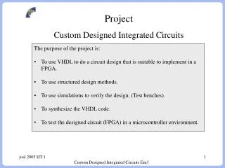
Project Custom Designed Integrated Circuits. The purpose of the project is: To use VHDL to do a circuit design that is suitable to implement in a FPGA. To use structured design methods. To use simulations to verify the design. (Test benches). To synthesize the VHDL code.

E N D
Project Custom Designed Integrated Circuits • The purpose of the project is: • To use VHDL to do a circuit design that is suitable to implement in a FPGA. • To use structured design methods. • To use simulations to verify the design. (Test benches). • To synthesize the VHDL code. • To test the designed circuit (FPGA) in a microcontroller environment. Custom Designed Integrated Circuits Em3
Project • The students can choose between these alternatives: • UART (Universal Asynchronous Receiver Transmitter) interfaced to a PIC16F84 microcontroller (later to MIPS). • VGA controller interfaced to PIC16F628 (later to MIPS) • If you are not a student from Em3 you can make your own choice of a project • The interface between the microcontroller and the project circuit is specified. • The program in the microcontroller is specified and implemented. Custom Designed Integrated Circuits Em3
DSUB9 MAX232 OSC DSUB15 FPGAXCS10 PIC16F84 JTAG REG + - IO-port Project, Test hard ware Custom Designed Integrated Circuits Em3
MAX232 DSUB9 OSC DSUB15 JTAG FPGAXCS10 PIC16F84 + - IO-port REG VGA-monitor Project, Test hardware Hyperterminal>? I2C slave Custom Designed Integrated Circuits Em3
Project • Design steps: • Design the selected circuit. • Design a test bench. • Verify the design. • Demonstrate the test bench simulations for the supervisor. • Synthesize the circuit and implement it in the test hardware. • Test the design. • Demonstrate the implemented design for the supervisor. • Write a project report and hand it over to the supervisor. Custom Designed Integrated Circuits Em3
Project • Assignment reports: • Demonstrate the test bench simulations for the supervisor. Every student must be prepared to demonstrate and explain the simulations and to describe the circuit design and the test bench. • Demonstrate the implemented design for the supervisor. • Write a project report and hand it over to the supervisor. • Passed exam for the project Gate Gate Gate Custom Designed Integrated Circuits Em3
Project UART --************************************************************* -- Project: uart -- clk: input clock 4 MHz. The same clock is used for FPGA and -- microcontroller. -- reset: internal signal in FPGA -- wr: write signal from micro. -- rd: read signal from the micro. dbus direction from FPGA to micro when -- ’1’. Statusreg or datareg on dbus when rd=’1’. -- a0-a1: register selection address lines -- dbus: bidirectonal data bus. (D0 to D7 in schematics) --************************************************************* entity uart is port(clk, reset, wr, rd, a0, a1: in std_logic; dbus: inout std_logic_vector(7 downto 0); end; Custom Designed Integrated Circuits Em3
Project --************************************************************* -- Project: uart -- duplex: full -- Bitrate: 9600 bits/s. Fix baudrate generator 4 MHz to 9600. -- Data bits: 8 -- Parity: even -- Stop bits: 2 -- Receiver: Oversampling 16 times -- Clock: 4 Mhz -- Address 0: Data register -- Address 1: Statusregister -- Address X: address 2-7 not used. -- Buffers: Only single buffers => write directly to transmit -- shift register and read directly from receive shift register. --************************************************************* Custom Designed Integrated Circuits Em3
Project start d0lsb d1 d2 d3 d4 d5 d6 d7msb par stop stop Micro FSM Receive Status Transmit Custom Designed Integrated Circuits Em3
Project Custom Designed Integrated Circuits Em3
clk data wr Project Custom Designed Integrated Circuits Em3
Project clk (micro and UART) WR synchronized WR data is latched in transmitter Custom Designed Integrated Circuits Em3
Project clk (micro and UART) RD dbus<=receivereg when rd=’1’ and a0=’0’ else statusreg when rd=’1’ and a0=’1’ else(others=>’Z’); Custom Designed Integrated Circuits Em3
Pattern and style in Project • Design methodology for project • Don’t build too small or too big entities. (In the project ca 3-5) • Max 4 levels in hierarchy. Structural VHDL is not so easy to understand. • Use state machines (required). Make models with ASM (Algorithmic State Machine) • Use variables only for temporary storage e.g. in algorithms. • Never use variables for e.g. registers. • Use patterns. Look for design examples. A state machine template is an example of a pattern that can improve the design and the readability. Custom Designed Integrated Circuits Em3
Project VGA Controller HSYNC x y VSYNC Cursor-sprite 8*8 Cursorpos(xc, yc) Custom Designed Integrated Circuits Em3
Project VGA Controller HSync Timing control clk VSync reset Blanking X(9 downto 0) Y(8 downto 0) Xbs(2 downto 0) Background sprite Spritecontrol PIC16F628 Ybs(2 downto 0) 6 DA 3 VGA C interface Xcs(2 downto 0) Cursor sprite Ycs(2 downto 0) Custom Designed Integrated Circuits Em3