Download
1 / 51
510 likes | 629 Views
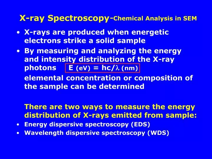
- Chemical Analysis in SEM. X-ray Spectroscopy. X-rays are produced when energetic electrons strike a solid sample By measuring and analyzing the energy and intensity distribution of the X-ray photons E (eV) = hc/ l (nm)

E N D
-Chemical Analysis in SEM X-ray Spectroscopy • X-rays are produced when energetic electrons strike a solid sample • By measuring and analyzing the energy and intensity distribution of the X-ray photons E (eV) = hc/l (nm) elemental concentration or composition of the sample can be determined There are two ways to measure the energy distribution of X-rays emitted from sample: • Energy dispersive spectroscopy (EDS) • Wavelength dispersivespectroscopy (WDS)
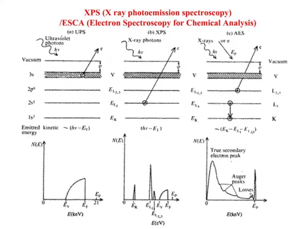
Principles of X-ray Production X-ray are produced by transitions of electrons between shells of atoms Shells correspond to particular energy level for an atom Transition between shells and energy levels are characteristicof element (20keV) 1. Ionization-excitation L Create a vacancy in K shell excited state K E-E 2. Relaxation-deexicitation E K L e- in L shell jumps in to fill vacancy K Auger Electron Emission nonradiative radiative L Process of inner-shell ionization and subsequent deexcitation
Excitation of K, L, M and N shells and Formation of K to M Characteristic X-rays M L K K2 K1 • If an incoming electron has sufficient kinetic energy for knocking out an electron of the K shell (the inner-most shell), it may excite the atom to an high-energy state (K state). • One of the outer electron falls into the K-shell vacancy, emitting the excess energy as a x-ray photon. • Characteristic x-ray energy: Ex-ray=Efinal-Einitial K I II III K L M N L subshells K state (shell) Energy K K L state K excitation L M state EK>EL>EM EK>EK M L excitation N state ground state
K emission spectrum of copper K K K K
Characteristic X-ray SpectrumYBaCuO6.9 Superconductor BaL1 BaL2 CuK BaL1 YK • As Z increases the Kth shell line energy increases (Y vs Cu). • If K-shell is excited,then all shells are excited (Y, Cu, Ba) • but they may not be detected. • Severe spectral overlap may occur for low energy lines.
EDS - Basics E (eV) = hc/l (nm) Si(Li) detector • In most of the modern EDS system, a semiconductor detector is used for measuring the energy of the x-ray photon emitted from the specimen. The X-ray energy is displayed as a histogram of number of photons versus energy. • Liquid nitrogen is for cooling the detector so as to reduce noise caused by thermal excitation. • A window is therefore required for protecting the detector against condensation when the sample chamber is opened. LN2 Be window specimen Owing to the use of Be window, only elements higher than Be can be detected.
X-ray Detector When an x-ray photon hits the detector, it ionizes the Si and generates a large number of electrons and holes. Electrons are then accelerated to the positive side (top) and holes to the negative side. Thus, a current pulse is generated and its magnitude is proportional to the x-ray energy. Requires liquid nitrogen cooling
EDS map of a sandstone Carbon Silicon Calcium Overlaying showing the distribution of carbon, silicon and calcium
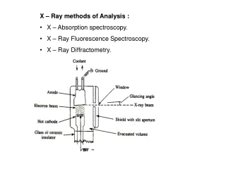
WDS - Basics E (eV) = hc/l (nm) Bragg’s Law:2d sin = 1 • A crystal of fixed d is moved along a circle to vary so that x-ray of different is recorded. • No window needed, therefore light elements can be detected • Peak very sharp • Very large S/Nratio c.f. EDS. 1 ~ 1 2 ~ 2 I 2 X-ray is diffracted by LiF crystal and detected by a proportional counter, and then amplified, processed. X-ray intensity is displayed as a function of l.
EDS vs WDS WDS EDS Spectra one element entire spectrum Acceptance per run in one shot Collection time tens of min mins Resolution ~a few eV ~130eV Probe size ~200nm ~5nm Max. Count rate ~50000 cps <2000 cps Detection limits 100ppm 1000ppm Accuracy ~4-5wt% ~4-5wt% Spectral artifacts rare peak overlap absorption etc. cps - count/second on an X-ray line
EDS vsWDS EDS FWHM=135-eV WDS FWHM=a few-eV Wavelength (nm) Superposed EDS and WDS spectra from BaTiO3. The EDS spectrum shows the strongly overlapped Ba La-Ti Ka and Ba Lb1-Ti Kb peaks. The WDS peaks are clearly resolved.
Quantitative Analysis – Thin Samples Cliff-Lorimer Technique Ca IA = Kab Cb IB Ca and Cb are weight fraction of element a and b IA and IB are the peak intensities Kab is a constant depending on the two elements and the operating conditions, and can be obtained by using a standard sample.
Orientation Imaging Microscopy (OIM) Electron backscatter diffraction patterns (EBSP) are obtained in SEM by focusing e- beam on a crystalline sample. Diffraction pattern is imaged on a phosphor screen and captured using a CCD camera. OIM is based on an automatic indexing of EBSP and provides a complete description of the crystallographic orientations in polycrystalline materials. Effects of the crystal orienta-tions on materials properties. Phosphor screen e- specimen EBSP
Applications of OIM • Orientation/misorientation • Physical properties are often orientation dependent • Young’s modulus, permeability, hardness, plasticity, etc. • Fatigue mechanism, creep in superalloys, integrity of single crystals, in-service reliability of microelectronic, corrosion, cracking, fracture, segregation and precipitation, twinning and recrystallization, etc. • Phase identification-coupled with chemical analysis • Distinguish between phases having similar chemistries • Distinguish between body-centered cubic and face centered cubic form, etc. • Strain • Strain in superalloys and aluminum alloys • Assessment of implantation damage in Si from Ge ions
Fast and Accurate Indexing of Any Crystal System Monoclinic Orthorhombic Hexagonal Cubic Tetragonal Triclinic Trigonal
OIM-Grain Boundary Maps Grain Boundary Map Orientation Map A Grain boundary Map can be generated by comparing the orientation between each pair of neighboring points in an OIM scan. A line is drawn separating a pair of points if the difference in orientation between the points exceeds a given tolerance angle. An Orientation Map is generated by shading each point in the OIM scan according to some parameter reflecting the orientation at each point. Both of these maps are shown overlaid on the digital micrograph from the SEM.
OIM-Semiconductors Effect of micro-texture on Mean Time to Failure (MTF) of inter-connect lines and thin films for semiconductor applications. Good film Bad film
Specimen Preparation • Remove all water, solvents, or other materials that could vaporize while in the vacuum. • Flat surface is required for BSE and OIM • Firmly mount all the samples. • Non-metallic samples, such as building materials, insulating ceramics, should be coated so they are electrically conductive. Metallic and conducting samples can be placed directly into the SEM.
Coating Techniques Sputter coater is used to coat insulating samples Au and Al – good for SE yield AuPd alloy – good for high resolution C – used if X-ray microanalysis is required Coating should have low granularity in order not to mask the underlying structure (<20nm thick).
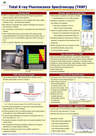
What is X-ray Fluorescence (XRF) The process of emissions of characteristic x-rays is called X-ray Fluorescence and analysis using x-ray fluorescence is called "X-ray Fluorescence Spectroscopy Main use Identification of elements; determi- nation of composition and thickness (for thin film samples) Samples Solids, powders and liquids; 5.0cm in diameter Range of elements All but low-Z elements: H, He, and Li Accuracy 1% composition, 3% thickness Detection limits 0.1% in concentration Depth sampled Normally in the 10nm range, but can be a few nm in the Total-reflection XRF (TXRF) Instrument cost $400K-$2.4M
XRMF-Basics • X-ray irradiates specimen • Specimen emits characteristic X-rays or XRF • Detector measures position and intensity of XRF peaks
XRMF Analysis - line scan A fast, convenient way to examine sample chemistry and heterogeneity along a line of analysis points. Ideal for studying diffusion profiles or layered materials. Line scan done on a printed circuit board
Elemental Mapping Qualitative Quantitative Spatial distribution Cu map Pb map
Scanning Probe Microscopy (SPM) • What is SPM? • Working principles of SPM • Basic components and their functions • Scanning Tunneling Microscopy (STM) • Scanning Force Microscopy (SFM) • Atomic force microscopy (AFM) • Advanced SPM techniques • Examples of SPM images
SPM Family Tree Invented at IBM by Gerd Binning and Heinrich Rohrer 2nm STM of silicon-Si(111) 7x7reconstruction
Applications of SPM To resolve a wide range of surface properties on the nanometer scale including: Topography, mechanical, magnetic, electric, thermal, and etc. e.g., DNA imaging, inspecting defects of semiconductors, measuring physical and chemical properties of surface. Advantages: Superior resolution and versatility of scanning probes Limitations: Long imaging times due to slow scanning speed The maximum imaging area is limited (<mm2)
Typical STM and AFM Modules Dimension 3100 AFM The world's best selling SPM The world's first truly flexible SPM, providing a single system that could meet all of the the needs of most scientists and engineers at an affordable price. Low temperature STM atomic resolution at 5K Cost: $500K(ambient) to $1.6M (ultrahigh vacuum)
How Does SPM Work? The SPM creates images with the sense of touch instead of light or electrons. Imagine drawing a picture of a computer keyboard without using your eyes. You could drag your fingertip over the surface to "feel" what the keyboard looks like. Instead of a fingertip, the SPM has a very tiny sensor called a probe. The SPM can magnify an object up to 10,000,000 times. In the laboratory under ideal conditions, the SPM can be used to look at individual atoms.
SPMs are used for studying surface topography and properties of materials from the atomic to the micron level. Schematic of a generalized SPM Probe Motion Sensor Probe Scanner Electronics Computer Vibration isolation
Basic Principles of SPM (STM & AFM) SPM relies on a very sharp probe positioned within a few nanometers above the surface of interest. When the probe translates laterally (scanning) relative to the sample, any change in the height of the surface causes the detected probe signal to change. A 3-D map of surface height is carried out with a probe scanning over the surface while monitoring some interaction between the probe and the surface. Probe signals that have been used to sense surfaces include electron tunneling current (STM), interatomic forces (van der Waals force, AFM), magnetic force (MFM), capacitive coupling (SCM), electrostatic force (EFM), and thermal coupling (SThM), etc. The probe signals depend so strongly on the probe-sample interaction that changes in substrate height of ~0.1Å can be detected with a sub-nm lateral resolution.
Basic SPM Components • Scanning System: Scanner - the heart of the microscope. It may scan the sample or the probe. A piezoelectric tube scanner can provide sub-Å motion increments. • Probe (tip): Very sharp tips are secured on • the end of cantilevers which have a wide • range of properties designed for a variety • of scanning probe technologies. There are • also many types of tips with varying shapes • for probing different morphologies and • scales of surface features and materials • (conducting, magnetized, very hard, etc.). • Probe Motion Sensor: Senses the • spacing between the probe and the • sample and provides a correction • signal to the piezoelectric scanner • to keep the spacing constant. The • common design for this function is • called beam deflection system as • shown at right figure.
Scanning Tunneling Microscope(STM) It=Ve-Cd STM uses a sharpened, conducting tip with a bias voltage applied between the tip and the sample. When the tip is brought within about 10Å of the sample, electrons from the sample begin to "tunnel" through the 10Å gap into the tip or vice versa, depending upon the sign of the bias voltage. tip V vacuum 90%It d~10Å sample It varies with tip-to-sample spacing and is also a function of local electronic structure or surface state. It is the signal used to create a STM image. For tunneling to take place, both the sample and the tip must be conductors or semiconductors.
Imaging of surface topology can be done in one of two ways: Two Scanning Modes in STM-2 Scan direction Tunneling current is monitored as the tip is scanned parallel to the surface. There is a periodic variation in the separation distance between the tip and surface atoms. A plot of the tunneling current v's tip position shows a periodic variation which matches that of the surface structure-a direct "image" of the surface. It It constant height mode Scan direction Tunneling current is maintained constant as the tip is scanned across the surface. This is achieved by adjusting the tip's height above the surface so that the tunneling current does not vary with the lateral tip position. The image is then formed by plotting the tip height v's the lateral tip position. It It constant current mode
Atomic Force Microscope (AFM) AFM senses interatomic forces that occur between a probe tip and a sample. a laser beam bounces off the back of the cantilever onto a photodiode. As the cantilever scans over a sample it bends and the position of the laser beam on the detector shifts. The cantilever deflection is regarded as the vertical force signal between the tip and the sample surface. The local height of the sample is measured by recording the vertical motionof the tip while keeping the cantilever deflection at constant. Photo diode detector Probe tip Piezoelectric sample scanner Optical lever detection of cantilever deflection 3-D topographical maps of the surface are then constructed by plotting the local sample height versus horizontal probe tip.
Silicon Nitride-Contact Mode AFM Probe Substrate Tip Cantilever Probes Spring constants (N/m) The properties and dimensions of the cantilever play an important role in determining the sensitivity and resolution of the AFM. cantilever
Contact, Non-Contact and TappingMode AFM Contact Non-contact Tapping Measure topography by a.Sliding the probe tip across surface b.Sensing Van der Waals attractive forces between surface and probe tip held above surface c.Tapping the surface with an oscillating probe tip c a b Contact mode imaging is heavily influenced by frictional and adhesive forces which can damage samples and distort image data. Non-contact imaging generally provides low resolution and can also be hampered by the contaminant layer which can interfere with oscillation.TappingMode imaging eliminates frictional forces by intermittently contacting the surface and oscillating with sufficient amplitude to prevent the tip from being trapped by adhesive meniscus forces from the contaminant layer.The graphs under the images represent likely image data resulting from the three techniques.
LiftMode AFM 2nd pass 1st pass Magnetic or electric Field source Lift height Topographic image Non-contact Force image LiftMode is a two-pass technique for measurement of magnetic and electric forces above sample surfaces. On the first pass over each scan, the sample's surface topography is measured and recorded. On the second pass, the tip is lifted a user-selected distance above the recorded surface topography and the force measurement is made.
Topographic structure (a) and Magnetic force image (b) of a compact disk a b Topographic structure results from surface preparation and exhibits striations from a polishing process (imaged using Tapping Mode) and magnetic force image (LiftMode and lift height 35nm) shows small magnetic domains that are unrelated to surface topography.
Image Insulating Surfaces at High Resolution in Fluid - AFM 18nm 1 2 Image of two GroES mole- cules positioned side-by- side in fluid, demonstra- ting 1nm lateral resolu- tion and 0.1nm vertical resolution. Entire molecule measures 84Å across and a distinct 45Å “crown” structure protrudes 8Å above remaining GroES surface. Fluid cell for an AFM which allows imaging in an enclosed, liquid environment.
Advanced SPM Techniques • Lateral Force Microscopy (LFM) measures frictional forces between the probe tip and the sample surface • Magnetic Force Microscopy (MFM) measures magnetic gradient and distribution above the sample surface; best performed using LiftMode to track topography • Electric Force Microscopy (EFM) measures electric field gradient and distribution above the sample surface; best performed using LiftMode to track topography • Scanning Thermal Microscopy (SThM) measures temperature distribution on the sample surface
Advanced SPM Techniques • Scanning Capacitance Microscopy (SCM) measures carrier (dopant) concentration profiles on semiconductor surfaces • Nanoindenting/Scratching measures mechanical properties of thin films and uses indentation to investigate hardness, and scratch or wear testing to investigate film adhesion and durability • Phase Imaging measures variations in surface properties (stiffness, adhesion, etc.) as the phase lag of the cantilever oscillation relative to the piezo drive and provides nanometer-scale information about surface structure often not revealed by other SPM techniques • Lithography Use of probe tip to write patterns
Examples of AFM Images 3-D Al2O3 10m 80nm tall elevated features in a Si/Si3N4 substrate 4m Grain growth studies Lateral force map of a patterned, monolayer, organic film deposited on a gold substrate. The strong contrast comes from the different frictional characteristics of the two materials. 30 µm scan.
Writing/Reading on Ferroelectric MaterialsAFM/Electric Force Microscopy (EFM) Mode : a. Initial surface was first imaged in non-contact mode without a bias voltage at the tip. b. Imaging of the same surface area yields both dark and bright spots indicating the presence of positive and negative gradients. c. Image was acquired with -1.5 V at the tip. The features appear black, due to a repulsive electro-static force interaction. d. The opposite contrast is observed here, where a positive bias of 1.5 V was applied to the cantilever tip. a b c d - + LaTiO3.5 polarization
Nanoindentation Using a diamond tip to indent a surface and immediately image the indentation. Using indentation cantilevers, it is possible to indent various samples with the same force in order to compare hardness properties. metal-foil diamond tip Indentations on two different diamond-like carbon films using three different forces (23, 34, and 45N) with four incidents made at each force to compare difference in hardness. 200nm Indentation depths are deeper for the softer thin film (right).
IC Failure Analysis and Defect Inspection with Scanning Thermal Microscopy a b a. Top-view image of surface topography of a failing IC where emission microscope detected two current leakage points but did not give the exact location of failure. The image shows no topographical features which suggest a problem. b. Scanning thermal microscopy (SThM) temperature distribution map of the same area showing a hot area on the surface above what was found to be a gate oxide short.
STM - Seeing Atoms STM image showing single-atom defect in iodine adsorbate lattice on platinum. 2.5nm scan Iron on copper (111)
Factors Influencing the Resolution of SPM • Broadening • Aspect ratio • Compression • Interaction forces Tip broadening arises when the radius of curvature of the tip is comparable with, or greater than, the size of the feature trying to be imaged. Tip Image Surface The aspect ratio (or cone angle) of a particular tip is crucial when imaging steep sloped features.