Download
1 / 23
290 likes | 596 Views
Semiconductor Innovatio n : Packaging and Test Kevin Suh HT Micron Semicondutores November 18 , 2010. Contents. 1. Innovation : “Breakthrough”. 2 . Global Semiconductor Backend. 3 . HT Micron and Packaging Technology. 4 . Innovation : “Breakthrough” in Brasil.

E N D
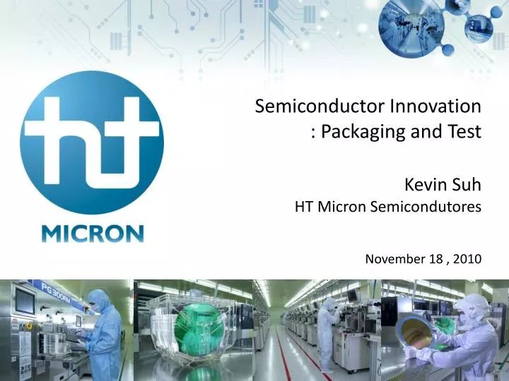
Semiconductor Innovation : Packaging and Test Kevin Suh HT Micron Semicondutores November 18 , 2010
Contents 1. Innovation : “Breakthrough” 2. Global Semiconductor Backend 3. HT Micron and Packaging Technology • 4. Innovation : “Breakthrough” in Brasil
1. Innovation : “Breakthrough” 2. Global Semiconductor Backend 3. HT Micron and Packaging Technology • 4. Innovation : “Breakthrough” in Brasil
Innovation : “Breakthrough” : an act or instance of breaking through an obstacle : a sudden advance especially in knowledge or technique
1. Innovation : “Breakthrough” 2. Global Semiconductor Backend 3. HT Micron and Packaging Technology • 4. Innovation : “Breakthrough” in Brasil
Semiconductor Packaging Technology Evolution (Source :Fujitsu)
Semiconductor Packaging Market After declining 14.7% in 2009, the semiconductor assembly and test service market will expand by 37% in 2010. Industry capacity utilization was above 85% by Q2, but has shown some signs of slowing over Q3. Semiconductor assembly and test service companies focus on advanced packaging and copper bonding capacity. Memory assembly and test capacity is being expanded. (Source :Gartner)
Components for Cellular Phones QFN for RF Various SOP SRAM Memory TSOP CDMA/GSM Controller & Graphics FCBGA QFP FBGA-SD3 PiP DIP
Components for Notebook Pwr Mgmt TO Memory Module Memory Controller & Graphics FCBGA QFP SRAM Memory TSOP QFN for RF Chipset PBGA Clock Control TSOP Pentium Processor FCBGA Various SOP
1. Innovation : “Breakthrough” 2. Global Semiconductor Backend 3. HT Micron and Packaging Technology • 4. Innovation : “Breakthrough” in Brasil
Flipchip+PiP+SiP Semiconductor Packaging Technology POP PiP uUSB–SiP SD8(1.5T) SiP/3D Hybrid CSP fc-PiP (1.4T) Flipchip + Stack SIP Flipchip+SiP uUSB Memory Hybrid WFBGA-SD4 0.8T 7D CSP 1.4T 8D CSP 1.4T VQFN-SD2 4DCSP 1.4 &1.2T 4D CSP 1.0T UFBGA-SD2 0.65T Stack WLCSP(0.5T) WFBGA(0.8T) fcBGA TFBGA(1.2T) Multi Row QFN S2-CSP(0.65T) Single ULGA(0.65T) BOC VFBGA(1.0T) fcCSP 1.0T QFN-SD TSOP-Quad Leaded TSOP-Quad-FU QFN TSOP-Double
“Thinner and Smaller” 0.35T FLGA XFLGA 0.55T 0.45T XFLGA UFLGA 0.6T 0.6T UFBGA 0.45T FBGA WFBGA 0.8T 0.5T FBGA-SD2 0.65T WFBGA-SD2 WFBGA-SD2 0.8T VFBGA-SD3 1.0T 0.8T WFBGA-SD3 VFBGA-SD4 1.0T 0.6T FBGA-SD4 0.8T WFBGA-SD4 TFBGA-SD4 1.2T uUSB-x16 uUSB-x8 uUSB-x4 1.5T MicroSD-x2 MicroSD-x4 MicroSD-x8 BOC-SD2 1.2T
System in Package (SIP) • Technology • - 50um wafer thinning(B/G, Saw) • 50um Thin die handling (D/A, WB) • Film Die attach(all FOW) • Reverse wire bonding Live Chip FOW Film 1.4mm thickness package Die thickness: 50µm (2 mils) 32Gb x 8 die = 32GB : 32 hours movie, MP3 8000 songs, 200 years newspaper
µUSB (SIP) – 16 die stack Live Chip WBL Film Max 1.6mm thickness package µUSB 11.3 x 24.8mm, 4LD Capacity: 4/8/16/32/64 GB PCB: 0.21mmT, 2Layer 1.34mm mold cap thickness Die thickness: 50µm (2mils) All Forward bonding Film D/A (All WBL film) • Application • NAND Flash Memory
Package on Package (POP) POP (PKG on PKG) [Top] FBGA-POP 15x15mm, 160LD Max. 1.1T Package Profile 0.21T +/- 0.03mm substrate Ni / Au 0.45 Mold Cap Thickness Solder ball 0.42mm SAC305 [Bottom] Substrate 0.3mm T 4L (1-2-1, Build Up, Ni/Au) Solder ball 0.3mm(SAC105) 0.5mm ball pitch • Application • Cell phone, PDA, Digital camera, MP3 player
Flip Chip SIP EMC FBGA Passive component Smallest in the world Flip chip-SiP & WLCSP embedded Module Bluetooth Class1 Large density with small form factor 10x10mm Package body size / 32LD Max.1.7mm Package profile 6-Layer, 0.5mm Build-up substrate Trench design with via-in pad 1.2T Mold cap thickness BC4 ROM CSP + 7 Active Discrete + 43RLC FC bonding with Pb-free WLCSP (0.30 ball, 0.50mm pitch) Underfill & Overmold process configuration ROHS & Green compliant Schematic Diagram Substrate Schematic Diagram Substrate FC die Passive Component RF SW Pwr Amp LNA X-tal SMT Underfill WLCSP E2PROM Balun filter
Protection One Chip (POC) Passives ; R,L,C • 1’st & 2’nd Gen.(~2010) • TSSOP 3.0x6.4 & TEP 2.0x6.0 • (AOS/Richo/Seiko) 2 IC in 1 PKGwith SOT type Protection IC MOS FET PCM (Protection Circuit Module) : 6.0 x 42.0 x 1.8mmt • 3’rd Gen.(~2011) • ESON 2.0x5.0x0.8t • (AOS/ITM/Hitachi/) 2 IC in 1 PKG with DFN type • 4’th Gen.(~2011) • DFN 2.0x3.5x0.5t • SiP-PCM • Replacing PCM SiP PCM 2.0 x 6.0 X 0.9mmt Li-ion Battery • 5’th Gen.(~2015) • SiP 4FLGA 2.0x6.0x0.8t
MCP (multi-chip packaging) & e-MMC e-MMC (Embedded Multi Media Card) JEDEC Standard e-MMC ver 4.4 Target Performance • Capacity : Up to 128GB • Read speed : 70MB/s , Write speed : 70MB/s
Product Portfolio of HT Micron FLASH: NAND FLASH, MCP, moviNAND, oneNAND, SSD, Flash Cards Cellular Phone Market : Samsung, LG, Motorola, SONY, HTC, Nokia • Imaging Solutions • Mobile DDI (Display Driver IC) • Mobile TV (ISDB-T) • Mobile SoC • Micro SD • MCP/oneNAND HOME APPLIANCES SMART CARD • Bluetooth, Zigbee • Panel DDI • Microcontroller • Media SoC
1. Innovation : “Breakthrough” 2. Global Semiconductor Backend 3. HT Micron and Packaging Technology • 4. Innovation : “Breakthrough” in Brasil
Innovation : “Breakthrough” in Brasil • All the efforts need to be coordinated for synergy • Resource planning is very important • Training human resources in various areas • All the efforts need to be aligned with policies • Semiconductor cluster physically and virtually Government Universities Market R&D Industry Institutes Industry
Inovação : “Breakthrough” emBrasil Let’s do it together