Download
1 / 12
160 likes | 289 Views
Field Effect Transistor. What is FET.

E N D
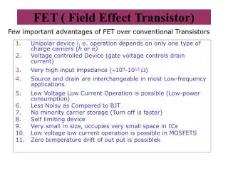
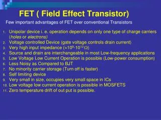
What is FET • FET is abbreviation of Field Effect Transistor. This is a transistor in which current is controlled by voltage only and no current is drawn. It is a high input impedance device and is used in computers, telecommunication and control circuits. This transistor is better in certain parameters as compared to BJT, that is Bipolar Junction Transistor.
A field-effect transistor (FET) is a type of transistor commonly used for weak-signal amplification (for example, for amplifying wireless signals). The device can amplify analog or digital signals. It can also switch DC or function as an oscillator.
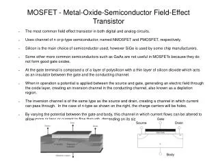
In the FET, current flows along a semiconductor path called the channel. At one end of the channel, there is an electrode called the source. At the other end of the channel, there is an electrode called the drain. The physical diameter of the channel is fixed, but its effective electrical diameter can be varied by the application of a voltage to a control electrode called the gate. The conductivity of the FET depends, at any given instant in time, on the electrical diameter of the channel. A small change in gate voltage can cause a large variation in the current from the source to the drain. This is how the FET amplifies signals.
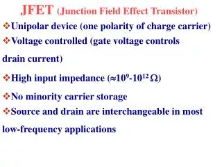
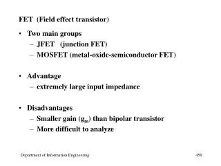
Classification of FET • Field-effect transistors exist in two major classifications. These are known as the junction FET (JFET) and the metal-oxide- semiconductor FET (MOSFET)
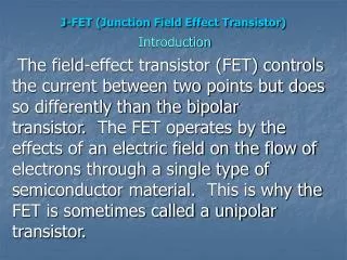
JFET • The junction FET has a channel consisting of N-type semiconductor (N-channel) or P-type semiconductor (P-channel) material; the gate is made of the opposite semiconductor type. In P-type material, electric charges are carried mainly in the form of electron deficiencies called holes. In N-type material, the charge carriers are primarily electrons. In a JFET, the junction is the boundary between the channel and the gate. Normally, this P-N junction is reverse-biased (a DC voltage is applied to it) so that no current flows between the channel and the gate. However, under some conditions there is a small current through the junction during part of the input signal cycle.
MOSFET • In the MOSFET, the channel can be either N-type or P-type semiconductor. The gate electrode is a piece of metal whose surface is oxidized. The oxide layer electrically insulates the gate from the channel. For this reason, the MOSFET was originally called the insulated-gate FET (IGFET), but this term is now rarely used. Because the oxide layer acts as a dielectric, there is essentially never any current between the gate and the channel during any part of the signal cycle. This gives the MOSFET an extremely large input impedance. Because the oxide layer is extremely thin, the MOSFET is susceptible to destruction by electrostatic charges. Special precautions are necessary when handling or transporting MOS devices.
Advantages / Disadvantages • The FET has some advantages and some disadvantages relative to the bipolar transistor. Field-effect transistors are preferred for weak-signal work, for example in wireless communications and broadcast receivers. They are also preferred in circuits and systems requiring high impedance. The FET is not, in general, used for high-power amplification, such as is required in large wireless communications and broadcast transmitters.
Field-effect transistors are fabricated onto silicon integrated circuit (IC) chips. A single IC can contain many thousands of FETs, along with other components such as resistors, capacitors, and diodes.
JFET Construction and Operation • A schematic representation of an n channel JFET is shown in Figure An n-type channel is formed between two p-type layers which are connected to the gate. Majority carrier electrons flow from the source and exit the drain, forming the drain current. The pn junction is reverse biased during normal operation, and this widens the depletion layers which extend into the n channel only (since the doping of the p regions is much larger than that of the n channel). As the depletion layers widen, the channel narrows, restricting current flow.
MOSFET Construction and Operation Figure 121:n-channel E FET structure • MOSFET transistors have metal gates which are insulated from the semiconductor by a layer of SiO2 or other dielectric. In enhancement type MOSFETs, the application of a gate voltage activates the channel (by inducing a layer of carriers between source and drain under the gate, Figure 121). In depletion type MOSFETs, there is a small strip of semiconductor of the same type as that of the source and drain, and the gate voltage can either reduce (by depleting carriers) or increase (by increasing carriers) the channel current (Figure 122). In an n channel MOSFET, the conducting channel exists in a p type substrate. . Note the additional B terminal on the substrate, which is often connected directly to the source Figure 122:n-channel D FET structure
JFET Characteristics • The circuit of Figure 123 will be used to study the JFET characteristics. The JFET is a nonlinear device. The voltage sources VGG and VDD will be adjusted. A graph of the JFET characteristics, iD versus vDS and iD versus vGS is shown in Figure 124.