Download
1 / 19
190 likes | 195 Views
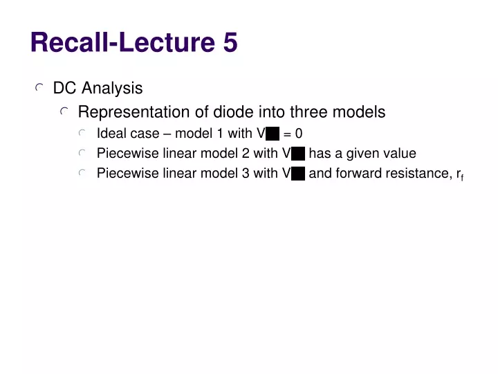
Recall-Lecture 5 . DC Analysis Representation of diode into three models Ideal case – model 1 with V = 0 Piecewise linear model 2 with V has a given value Piecewise linear model 3 with V and forward resistance, r f. Diode AC equivalent model

E N D
Recall-Lecture 5 • DC Analysis • Representation of diode into three models • Ideal case – model 1 with V = 0 • Piecewise linear model 2 with V has a given value • Piecewise linear model 3 with V and forward resistance, rf
Diode AC equivalent model • During analysis, must perform DC analysis first to calculate ID in order to obtain rd
DC ANALYSIS AC ANALYSIS DIODE = MODEL 1 ,2 OR 3 DIODE = RESISTOR, rd CALCULATE rd CALCULATE DC CURRENT, ID CALCULATE AC CURRENT, id
Other Types of Diodes The term ‘photo’ means light. Hence, a photodiode converts optical energy into electrical energy. The photon energy breaks covalent bond inside the crystal and generate electron and hole pairs Photodiode Solar cell converts visible light into electrical energy. The working principle is the same as photodiode but it is more towards PROVIDING the power supply for external uses Solar Cell
Light Emitting Diode An LED is opposite of photodiode this time, it converts electrical energy into light energy – Normally GaAs is used as the material for LED. During diffusion of carriers – some of them recombines and the recombination emits light waves. Schottky Barrier Diode A Schottky Barrier diode is a metal semiconductor junction diode. The metal side is the anode while the n-type is the cathode. But the turn on voltage for Schottky is normally smaller than normal pn junction diode
Breakdown Voltage • The breakdown voltage is a function of the doping concentrations in the n- and p-region of the pn junction. • Large doping concentrations result in smaller break-down voltage. • Reverse biased voltage – ET • The electric field may become large enough for the covalent bond to break, causing electron-hole pairs to be created. • So, electrons from p-type are swept to n-region by the electric field and holes from the n-type are swept to the p-region • The movement will create reverse biased current known as the Zener Effect.
Zener Effect and Zener Diode • The applied reverse biased voltage cannot increase without limit since at some point breakdown occurs causing current to increase rapidly. • The voltage at that point is known as the breakdown voltage, VZ • Diodes are fabricated with a specifically design breakdown voltage and are designed to operate in the breakdown region are called Zener diodes. Circuit symbol of the Zener diode: NOTE: When a Zener diode is reverse-biased, it acts at the breakdown region, when it is forward biased, it acts like a normal PN junction diode • Such a diode can be used as a constant-voltage reference in a circuit. • The large current that may exist at breakdown can cause heating effects and catastrophic failure of the diode due to the large power dissipated in the device. • Diodes can be operated in the breakdown region by limiting the current to a value within the capacities of the device.
e e e e atom atom atom h h h • Avalanche Effect • While these carriers crossing the space-charge region, they also gain enough kinetic energy. • Hence, during collision with other atoms, covalent bond is broken and more electron-holes pairs are created, and they contribute to the collision process as well. Refer to figure below Electron with high kinetic energy
Zener Diode 10 k Calculate the value of the current ID if VZ = 10V ANSWER: ID = 0.2 mA
The Zener diode with VZ = 4.7V is used in the circuit shown below and the input signal is a 20 V peak-to-peak square wave. Use V = 0 V Sketch the output signal, vo. + Vo - + Vin - R HINT: When a Zener diode is reverse-biased, it acts at the breakdown region, when it is forward biased, it acts like a normal PN junction diode
Voltage Regulator - Zener Diode A voltage regulator supplies constant voltage to a load.
3. The remainder of VPS drops across Ri 2. The load resistor sees a constant voltage regardless of the current 1. The zener diode holds the voltage constant regardless of the current • The breakdown voltage of a Zener diode is nearly constant over a wide range of reverse-bias currents. • This make the Zener diode useful in a voltage regulator, or a constant-voltage reference circuit.
Example A Zener diode is connected in a voltage regulator circuit. It is given that VPS = 20V, the Zener voltage, VZ = 10V, Ri = 222 and PZ(max) = 400 mW. Determine the values of IL, IZand II if RL = 380 . Determine the value of RL that will establish PZ(max) = 400 mW in the diode.
For proper function the circuit must satisfied the following conditions. The power dissipation in the Zener diode is less than the rated value When the power supply is a minimum, VPS(min), there must be minimum current in the zener diode IZ(min), hence the load current is a maximum, IL(max), When the power supply is a maximum, VPS(max), the current in the diode is a maximum, IZ(max), hence the load current is a minimum, IL(min) Or, we can write AND
For general thumb of rule for design this circuit is, so from the last Equation Maximum power dispassion in the Zener diode is EXAMPLE Consider voltage regulator is used to power the cell phone at 2.5 V from the lithium ion battery, which voltage may vary between 3 and 3.6 V. The current in the phone will vary 0 (off) to 100 mA(when talking). Calculate the value of Riand the Zener diode power dissipation simple Zener diode voltage regulator circuit
Solution: The stabilized voltage VL = 2.5 V, so the Zener diode voltage must be VZ = 2.5 V. The maximum Zener diode current is The maximum power dispassion in the Zener diode is The value of the current limiting resistance is
Example 2 Range of VPS : 10V– 14V RL = 20 – 100 VZ = 5.6V Find value of Ri and calculate the maximum power rating of the diode