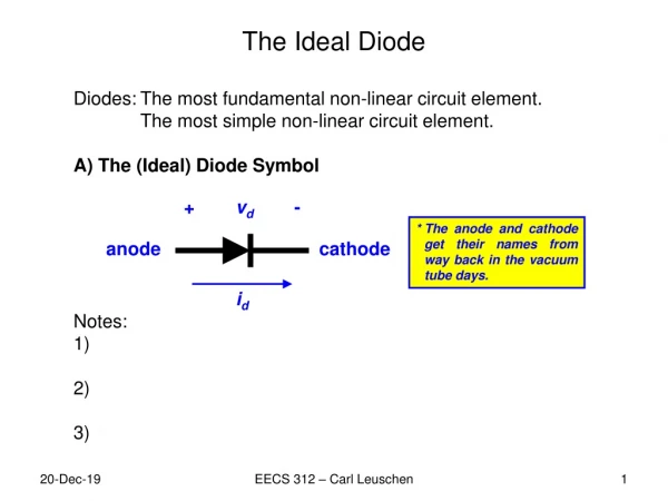
Download
1 / 24
300 likes | 1.09k Views
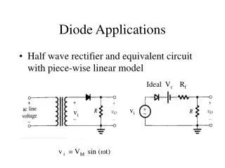
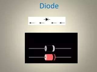
Ideal Diode Model. Let’s begin with an ideal diode and look at its characteristics. Real PN Junction Diode I-V Characteristic. •Typical PN junction diode I-V characteristic is shown on the right.

E N D
Let’s begin with an ideal diode and look at its characteristics
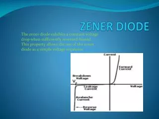
Real PN Junction Diode I-V Characteristic •Typical PN junction diode I-V characteristic is shown on the right. –In forward bias, the PN junction has a “turn on” voltage based on the “built-in” potential of the PN junction. The turn on voltage is typically in the range of 0.5V to 0.8V –In reverse bias, the PN junction conducts essentially no current until a critical breakdown voltage is reached. The breakdown voltage can range from 1V to 100V. Breakdown mechanisms include avalanche and zener tunneling.
Current Equations •The forward bias current is closely approximated by • where VT is the thermal voltage (~25.8mV at room temp T= 300K or 27C ) • k = Boltzman’s constant = 1.38 x 10⁻²³joules/kelvin • T = absolute temperature • q = electron charge = 1.602 x 10⁻¹⁹coulombs • n = constant dependent on structure, between 1 and 2 (we will assume n = 1) • IS= scaled current for saturation current that is set by diode size • –Notice there is a strong dependence on temperature • –We can approximate the diode equation for i>> IS •In reverse bias (when v << 0 by at least VT), then •In breakdown, reverse current increases rapidly…a vertical line
Mobile Carriers •Now let’s look at physical mechanisms from which the current equations come. –We’ve seen that holes and electrons move through a semiconductor by two mechanisms –drift and diffusion –In equilibrium, diffusion current (ID) is balanced by drift current (IS). So, there is no net current flow. Drift current comes from (thermal) generation of electron-hole pairs (EHP).
Band Diagrams •When the P-type material is contacted with the N-type material, the Fermi levels must be at equilibrium. •Band bending: The conduction and valence bands “bend” to align the Fermi levels. •Electrons diffuse from the N-side to the P-side and recombine with holes at the boundary. Holes diffuse from the P-side to the N-side and recombine with electrons at the boundary. There is a region at the boundary of charged atoms –called the space-charge region (also called the depletion region b/c no mobile carriers in this region) •An electric field is created which results in a voltage drop across the region –called the barrier voltage or built-in potential
What happens when P-type meets N-type? Holes diffuse from the p-type into the n-type, electrons diffuse from the n-type into the p-type, creating a diffusion current. The diffusion equation is given by Once the holes [electrons] cross into the n-type [p-type] region, they recombine with the electrons [holes]. •This recombination “strips” the n-type [p-type] of its electrons near the boundary, creating an electric field due to the positive and negative bound charges. •The region “stripped” of carriers is called the space-charge region, or depletion region. •V0is the contact potential that exists due to the electric field. •Some carriers are generated (thermally) and make their way into the depletion region where they are whisked away by the electric field, creating a drift current.
E-field and Built-in Potential •Diffusion is balanced by drift due to bound charges at the junction that induce an E-field. •Integrating the bound charge density gives us the E-field Integrating the E-field gives the potential gradient
Junction Built-In Voltage •With no external biasing, the voltage across the depletion region is: –Typically, at room temp, V0is 0.6~0.8V •How does V0 change as temperature increases? –Note that there is no measurable potential difference between the n-type and p-type materials of pn junction when in equilibrium. The electrochemical potentials (Fermi levels) are the equal.
Width of Depletion Region •The depletion region exists on both sides of the junction. The widths in each side is a function of the respective doping levels. Charge-equality gives: •The width of the depletion region can be found as a function of doping and the built-in voltage… esis the electrical permittivity of silicon = 11.7ε0 (where ε0 = 8.854E-14 F/cm)
Pn Junction in Reverse Bias (1) •As the depletion region grows, the capacitance across the diode changes. –Treating the depletion region as a parallel plate capacitor…
Reverse Bias (2) •Reverse bias: apply a negative voltage to the p-type, positive to n-type. •Increase the built-in potential, increase the barrier height. •Decrease the number of carriers able to diffuse across the barrier. •Diffusion current decreases. •Drift current remains the same (due to generation of EHP). •Almost no current flows. Reverse leakage current, IS, is the drift current, flowing from n to p.
Reverse Breakdown •Zener Breakdown: The bands bend so much that carriers tunnel through the depletion region. This will occur in heavily doped junctions when the n-side conduction band appears opposite the p-side valence band. •Avalanche Breakdown: carriers have enough energy to ionize an electron-hole-pair (EHP), creating more highly energetic carriers, which collide to form more EHPs, which creates…
pn Junction in Forward Bias (1) •Now let’s look at the condition where we push current through the pn junction in the opposite direction. –Add more majority carriers to both sides shrink the depletion region lower V0diffusion current increases •Look at the minority carrier concentration… –lower barrier allows more carriers to be injected to the other side •Note that np0= ni2/NA and pn0= ni2/ND –This comes from two equations…
•The forward bias voltage causes excess minority carriers to be injected across the junction. •The distribution of excess minority hole concentration in the n-type Siis an exponentially decaying function of distance from xn –where Lpis the diffusion length (steepness of exponential decay) and is set by the excess-minority-carrier lifetime, tp. The average time it takes for a hole injected into the n region to recombine with a majority carrier electron –The diffusion of holes leads to the following current density vs. x
•In equilibrium, as holes diffuse away, they must be met by a constant supply of electrons with which they recombine. Thus, the current must be supplied at a rate that equals the concentration of holes at the edge of the depletion region (xn). Thus, the current due to hole injection is: •Current due to electrons injected into the p region is… •Combined…
Minority Carrier Concentration and Current Densities in Forward Bias •Current is due to the diffusion of holes and electrons. Current is dominated by holes or electrons depending on the relative doping of NA vs. ND •Is NA> ND or NA<ND in this example?
Forward Bias (2) •Forward bias: apply a positive voltage to the p-type, negative to n-type. •Decrease the built-in potential, lower the barrier height. •Increase the number of carriers able to diffuse across the barrier •Diffusion current increases •Drift current remains the same •Current flows from p to n
Review of Biasing •Applying a bias adds or subtracts to the built-in potential. •This changes the diffusion current, making it harder or easier for the carriers to diffuse across. •The drift current is essentially constant, as it is dependent on temperature.
Photodiodes •Diodes have an optical generation rate. Carriers are created by shining light with photon energy greater than the bandgap. •Photodetector: should have large depletion widths and long diffusion lengths (minority carrier lifetimes) so that photo generatedEHPscan be collected and swept across the junction. •Solar Cell: operating in the fourth quadrant generates current, though small.
Light Emitting Diodes •When electrons and holes combine, they release energy. •This energy is often released as heat into the lattice, but in some materials, known as direct bandgap materials, they release light. •Engineering LEDs can be difficult, but has been done over a wide range of wavelengths. •This illustration describes the importance of the plastic bubble in directing the light so that it is more effectively seen.
Diode Circuits •Look at the simple diode circuit below. We can write two equations:
Diode Small-Signal Model •Some circuit applications bias the diode at a DC point (VD) and superimpose a small signal (vd(t)) on top of it. Together, the signal is vD(t), consisting of both DC and AC components –Graphically, can show that there is a translation of voltage to current (id(t)) –Can model the diode at this bias point as a resistor with resistance as the inverse of the tangent of the i-v curve at that point –And if vd(t) is sufficiently small then we can expand the exponential and get an approximate expression called the small-signal approximation (valid for vd< 10mV) –So, the diode small-signal resistance is…
•Perform the small signal analysis of the diode circuit biased with VDD by eliminating the DC sources and replacing the diode with a small signal resistance–The resulting voltage divider gives: •Separating out the DC or bias analysis and the small-signal analysis is a technique we will use extensively