Download
1 / 29
330 likes | 873 Views
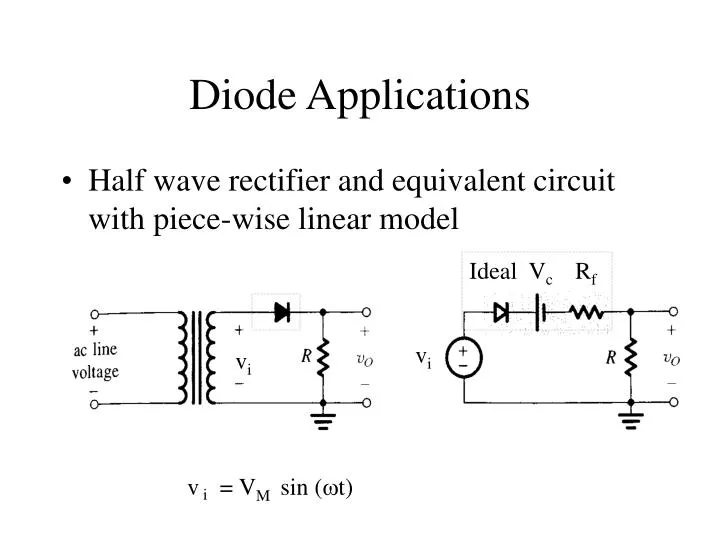
Ideal V c R f. v i. v i. Diode Applications. Half wave rectifier and equivalent circuit with piece-wise linear model. v i = V M sin ( t). Half Wave Rectifier. We initially consider the diode to be ideal, such that V C =0 and R f =0. Half Wave Rectifier.

E N D
Ideal Vc Rf vi vi Diode Applications • Half wave rectifier and equivalent circuit with piece-wise linear model v i = VM sin (t)
Half Wave Rectifier • We initially consider the diode to be ideal, such that VC =0 and Rf =0
Half Wave Rectifier • The (ideal) diode conducts for vi >0and since Rf =0 v0 vi • For vi < 0the (ideal) diode is an open circuit (it doesn’t conduct) and v0 0.
The diode must withstand a peak inverse voltage of V M Half Wave Rectifier • In this simplified (ideal diode) case the input and output waveforms are as shown
Half Wave Rectifier • The average d.c. value of this half-wave-rectified sine wave is
Half Wave Rectifier • So far this rectifier is not very useful. • Even though the output does not change polarity it has a lot of ripple, i.e. variations in output voltage about a steady value. • To generate an output voltage that more closely resembles a true d.c. voltage we can use a reservoir or smoothing capacitor in parallel with the output (load) resistance.
Smoothed Half Wave Rectifier Circuit with reservoir capacitor Output voltage The capacitor charges over the period t1 to t2 when the diode is on and discharges from t2 to t3 when the diode is off.
Smoothed Half Wave Rectifier • When the supply voltage exceeds the output voltage the (ideal) diode conducts. During the charging period (t1 <t< t2) vo = VM sin (t) (The resistance in the charging circuit is strictly Rf which we have assumed to be zero. Even for a practical diode RfC will be very small)
Smoothed Half Wave Rectifier • When the supply voltage falls below the output voltage the diode switches off and the capacitor discharges through the load. • During the discharge period (t2<t< t3 ) and vo = VM exp {- t’/RC} where t’= t- t2 • At time t3 the supply voltage once again exceeds the load voltage and the cycle repeats
Smoothed Half Wave Rectifier • The resistance in the discharge phase is the load resistance R. • RC can be made large compared to the wave period. • The change in output voltage (or ripple) can then be estimated using a linear approximation to the exponential discharge.
Smoothed Half Wave Rectifier • vo = VM exp {- t’/RC} VM [ 1- (t’/RC)] • The change in voltage V is therefore approximately given by VM t’/RC • For a the half wave rectifier this discharge occurs for a time (t3- t2 ) close to the period T = 1/f, with f= frequency. • Giving the required result:
Smoothed Half Wave Rectifier • We can define a ripple factor as where Vd.c. = (VM - V/2) The lower the ripple factor the better
Half Wave Rectifier • If we don’t consider the diode to be ideal then from the equivalent circuit we obtain, for vi >Vc: vi – Vc – i Rf - iR =0 i.e. • Giving
VM Non-Ideal Half Wave Rectifier
R/(R + Rf) VC vi Non-Ideal Half Wave Rectifier • A plot of v0against vi is known as the transfer characteristic
Non-Ideal Half Wave Rectifier • We usually have R>> Rf so that Rf can be neglected in comparison to R. • Often VM >> Vc so Vc can also be neglected. The transfer characteristic then reduces to v0 vi
vi Full-Wave (Bridge) Rectifier • We initially consider the diodes to be ideal, such that VC =0 and Rf =0 • The four-diode bridge can be bought as a package
vi Full-Wave (Bridge) Rectifier • During positive half cycles vi is positive. • Current is conducted through diodes D1, resistor R and diode D2 • Meanwhile diodes D3 and D4 are reverse biased.
vi Full-Wave (Bridge) Rectifier • During negative half cycles vi is negative. • Current is conducted through diodes D3, resistor R and diode D4 • Meanwhile diodes D1 and D2 are reverse biased.
Current always flows the same way through the load R. Show for yourself that the average d.c. value of this full-wave-rectified sine wave is VAV = 2VM/ (i.e. twice the half-wave value) Full-Wave (Bridge) Rectifier
Full-Wave (Bridge) Rectifier • Two diodes are in the conduction path. • Thus in the case of non-ideal diodes vo will be lower thanvi by 2VC. • As for the half-wave rectifier a reservoir capacitor can be used. In the full wave case the discharge time is T/2 and
Diode Clipper Circuits • These circuits clip off portions of signal voltages above or below certain limits, i.e. the circuits limit the range of the output signal. • Such a circuit may be used to protect the input of a CMOS logic gate against static.
Diode Clipper Circuits • When the diode is off the output of these circuits resembles a voltage divider
Diode Clipper Circuits • If RS << RL • The level at which the signal is clipped can be adjusted by adding a d.c. bias voltage in series with the diode. v0 vi
Diode Clipper Circuits • Let’s look at a few other examples of clipper circuits.
Diode Clamper Circuits • The following circuit acts as a d.c. restorer. • see Q9, example sheet1.
Diode Clamper Circuits • A bias voltage can be added to pin the output to a level other than zero.